ARINIC429 bus test device
Introduction to ARINIC429 Aviation Bus
The ARINIC429 bus is an aviation bus widely used by business aircraft in the 1980s. Its information content integrates more than 200 aviation parameters, mainly to solve the point-to-point data interaction in aviation equipment.
ARINIC429 bus data encoding method can be divided into binary data encoding (BNR) and binary to decimal 8421 encoding (BCD), using 32-bit bipolar non-recursive "1" "0", of which the highest 32 bits are parity check Bits, plus 4 silence interval bits at the end of each frame, the code rate is divided into 100Kbps and 12.5Kbps. Under normal circumstances, the receiver level is + 6V. + 5V ~ + 13V is regarded as logic "high"; -6.5V ~ -13V is regarded as logic "low"; -2.5V ~ + 2.5V is regarded as logic "empty", which is the data invalid state.
Each frame of ARINIC429 data is composed of five parts, namely: label (LABEL), identifier (SDI), data field (DATA), symbol matrix status bit (SSM) and parity bit (P). The specific meaning is:
Label (LABEL): ARINIC429 bus data specifies a constant label for each aviation parameter, such as the vacuum speed label is always 230.
Identifier (SDI): Identifies what data source the data comes from and which destination device it is sent to.
Data field (DATA): It is used to specify the parameter value and is filled with BCD or BNR code.
Symbol matrix status bit (SSM): describes the data attributes and the working status of the sending device.
Parity (P): Odd parity of ARINIC429 data.
Hardware design instructions
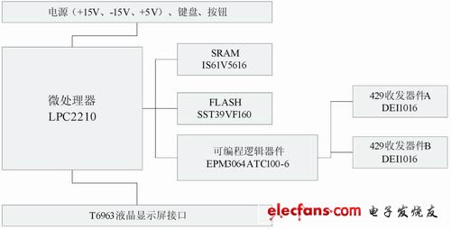
Figure 1 shows the block diagram of the ARINIC429 bus receiving and testing device. The entire device is designed with two ARINIC429 bus receiving and sending channels. You can send 2 ARINIC429 signals at the same time, interrupt receiving 4 ARINIC429 signals.

Figure 1 Block diagram of the receiving test device
The core processor of the device adopts LPC2210 with ARM7T core. LPC2210 has an open external bus structure and JTAG download debugging simulation function, supports ADS1.2 development environment simulation download, which greatly facilitates the user's development of actual products. The chip integrates 16K of RAM and is packaged in a 144-pin LQPF. Peripheral 3.3V power supply, nuclear voltage 1.8V. Interface buses such as I2C, PWM and UART are also integrated externally.
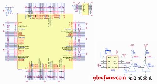
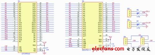
As shown in Figure 2, the LPC2210 uses a 11.0592MHz crystal oscillator. After the internal PLL control register, the frequency multiplier becomes the clock frequency above 60MHz. A 4Mb SRAM (IS61VL25616 addressing Ox80000000-Ox8007ffff) and a 16Mb FLASH (SST39VF160 addressing Ox81000000-Ox811fffff) are configured on the external storage bus. In order to facilitate debugging, the CE0 and CE1 chip selects of the LPC2210 have added jumpers. As shown in Figure 3. When debugging, the program code is mapped to the off-chip SRAM to run. After the product is finalized, the program is solidified to the off-chip FLASH to run. The bus width BOOT [1: 0] of the system is controlled by jumpers.

Figure 2 Partial block diagram of LPC2210 processor

Figure 3 Schematic diagram of an external storage device
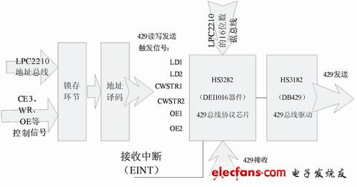
The entire ARINIC429 transmission link consists of HS3182 and HS3282 devices to form an ARINIC429 transceiver channel. HS3282 is the protocol chip of ARINIC429, HS3182 is the driver chip of ARINIC429 physical layer, and needs a differential voltage of ± 15V when working. LPC2210 addresses the data line and address line of the processor through a piece of programmable logic device EPM3064ATC100-6, and accesses the external HS3282 chip. Because the LPC2210 pin interface voltage is + 3.3V, and the I / O pin voltage of other peripheral devices such as programmable logic devices is + 5V, each pin is connected in series with a 470W resistor for circuit protection. The specific logic design of EPM3064ATC100-6 is shown in Figure 4.

Figure 4 HS3282 logic control block diagram
The LPC2210 chip select CE3 is used as the latch control signal of the address, and the logic decoding starts after the address passes the latch. Make the key control signals such as CWSTR (command word read and write), LD1, LD2 (transmit enable) of HS3282 effective respectively, and complete the timing enable operation for ARINIC429 sending and receiving. The LPC2210 data bus directly connects to the data line of the HS3282. In addition, EPM3064ATC100-6 also divides an external 4MHz clock source into two 1MHz clocks for the HS3282 chip. HS3282 sends a signal with TTL level to drive HS3182, and raises the signal voltage to meet the standard required by ARINIC429 bus. HS3182 needs + 15V, -15V voltage when working.
Outdoor Power Supply(300W 530Wh)
Outdoor power supply, also known as portable energy storage battery, is a device that uses high energy density lithium-ion battery pack as a means of energy storage to provide power supply for users when they are unable to access power. Outdoor power supply can provide power support for almost all electrical equipment. It has larger capacity, supports 220V AC output, USB fast charging output, vehicle cigarette lighter output port, DC output port, lighting flashlight, and even wireless charger and other functions, so as to provide users with more ways of power security as far as possible.
energy storage, power supply, lithium-ion battery, portable lithium battery, DC AC output
Wolong Electric Group Zhejiang Dengta Power Source Co.,Ltd , https://www.wldtbattery.com
