Comparison of image stabilization methods for mobile and consumer applications and ON Semiconductor's optical image stabilization solutions
Nowadays, people are shooting more and more through smartphones, tablets, digital cameras, video cameras and even cars. In the process of camera shooting, image jitter is often encountered. A typical example of jitter is when people shake their hands when they control the camera, which makes the image shake and makes it difficult to view, especially when the zoom function is fully zoomed in. In addition, the camera and camcorder will blur when capturing images while moving. Therefore, designers need to adopt appropriate image stabilization methods to help control jitter and blur when taking pictures and videos, and optimize the user experience.
There are currently three main image stabilization methods used in mobile, consumer, and automotive applications, including digital image stabilization (DIS), electronic image stabilization (EIS), and optical image stabilization (OIS). The main difference between DIS and EIS is the motion detection method. DIS uses a pixel mapping method, as shown in Figure 1. The DIS method places the dog in the middle by analyzing the picture. In other words, the pixel mapping method uses software to readjust the dog's position.
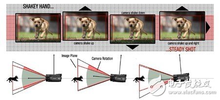
Figure 1. Digital image stabilization (DIS) uses a pixel mapping method to stabilize the image through software.
In comparison, EIS uses a gyroscope to detect camera motion and compensate for motion in real time, improving pixel and image quality to the highest. Both methods provide motion compensation by cropping the image. Since EIS uses a gyroscope to sense motion, EIS sensing accuracy is excellent, but because it still relies on cropping the image for motion compensation, the image quality is degraded. In Figure 2, you can see how the guard band is used to crop the image to compensate for jitter.
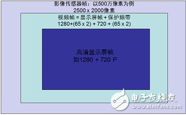
Figure 2. Electronic Image Stabilization (EIS) uses a gyroscope to detect camera motion and compensate.
Most applications use an application processor (AP) to process video or signals, including applications that use EIS and DIS. Especially DIS requires more processor resources to compensate for jitter and motion. In video applications, video compression is equivalent to image quality. When methods such as DIS and EIS require cropping, the quality of the image will decline, because the quality of the captured image must be continuously reduced and improved.
In comparison, the OIS method captures and uses the largest pixels, and does not need to reduce / improve the image quality through the guard band, so it provides maximum compression and optimizes the image quality. And because OIS provides internal compensation, it does not require any other application processor resources.
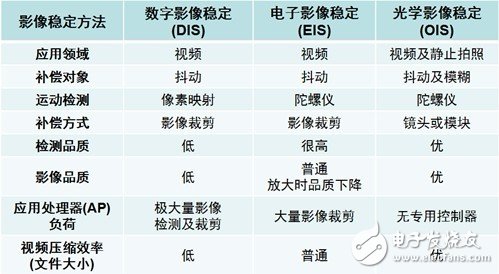
Table 1. Comparison of various image stabilization methods.
Other advantages of the OIS method
In addition, the unique OIS method also provides a greatly improved shutter speed and optimized exposure compensation up to 3 levels, much higher than other methods used. The OIS scheme usually consists of some major components, including an image sensor to determine the focal length, a gyroscope to compensate for motion, and optical image stabilization. These components can be assembled in a small space, using some standard design wiring.
OIS usually also integrates an open-loop or closed-loop autofocus design. Open-loop autofocus uses springs to provide resistance to lens stretching, and requires continuous power to resist lens stretching and keep it in position. By using a closed-loop autofocus system, you do n’t need a spring and continuous power to maintain the autofocus lens position. Since the position is known, less power is required to maintain the focus of the application. In a closed-loop AF system, the related power required in macro mode is no more than infinity. This also has a significant impact on the settling time required by each system. Because the typical open-loop AF takes time to stabilize, and then you have to continue to re-adjust. The time depends on the algorithm used, but it usually takes some time for the open-loop AF to stabilize. The closed-loop autofocus system uses a position sensor to determine the lens position, which can speed up the stabilization time to complete focusing.
ON Semiconductor's rugged and energy-efficient optical image stabilization solution
ON Semiconductor has developed a solution that combines these best possible features, namely the LC8981xx series of optical image stabilization controllers and drivers, including LC898111, LC898119 and LC898122. Among them, LC898111AXB-MH is a new OIS solution launched by ON Semiconductor. It is currently the industry's most accurate optical image stabilization controller and driver, which is used in applications such as smartphone camera modules. LC898111AXB-MH provides industry-leading accuracy and low energy consumption in a compact size (2.57 x 3.22 x 0.69 mm). The size of LC8981119 is further reduced to 2.0mm X 2.0mm X 0.675mm, and it provides extremely low energy consumption. Samples are now available. LC898122 further integrates closed-loop autofocus to provide a more powerful solution.
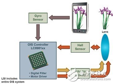
Figure 3. ON Semiconductor LC8981xx series optical image stabilization control and driver working schematic.
Figure 3 shows the working diagram of ON Semiconductor LC8981xx series. During initialization, this series of solutions will make the lens in the center position. The gyro sensor will detect the angular rate disturbance caused by hand shake, and the OIS controller will compensate for the instability by converting the angular rate into a travel distance and using it as a reference signal. The controller is assisted by the actuator Move the lens down and use a Hall sensor to detect the distance moved to provide feedback.
Taking the LC898111AXB-MH as an example, this new device combines the controller and driver functions required to handle OIS in a smartphone camera module. The significantly improved shutter speed makes exposure compensation far superior to competing OIS solutions. Therefore, it can achieve precise suppression control of camera shake. In addition, it can also be used to realize the indispensable left-right and up-down adjustment functions when walking and shooting. The output of this IC's integrated pulse width modulation (PWM) driver reduces energy consumption and reduces the impact of noise on image quality. This highly integrated, pre-programmed IC allows engineers to minimize the number of external components required in the system design, thereby reducing total energy consumption and board area.
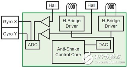
Figure 4. LC898111AXB-MH block diagram.
LC898111AXB-MH has built-in various digital and analog audio processing mechanisms, including dual-channel position sensing circuit, gyro filter interface circuit and lens servo circuit. The position sensing circuit includes a Hall amplifier circuit, a constant current digital-to-analog converter (DAC), a gain control operational amplifier, and a 12-bit analog-to-digital converter (ADC) for each channel. The gyro filter interface circuit is fully compatible with analog and digital signals. The gyro filter interface and lens servo circuit can be adjusted through the I2C and SPI bus interfaces, and can provide various corresponding configurations when connecting different gyros and actuators. Therefore, this device can cover a wider range of jitter frequency and thus provide a larger image stabilization angle.
ON Semiconductor built a demonstration device based on LC898111AXB-MH. Comparative tests show that when ON Semiconductor's OIS solution is enabled, the image becomes more stable and smooth without affecting image quality. (See the demo video for details)
to sum up:
Mobile and consumer applications require effective image stabilization solutions to control jitter and blurring, and thus optimize the user experience. ON Semiconductor ’s LC8981xx series of optical image stabilization solutions provide superior performance to digital image stabilization and electronic image stabilization in a very small size, and provide extremely low energy consumption, making them ideal for applications such as smartphones, tablets, and cameras.
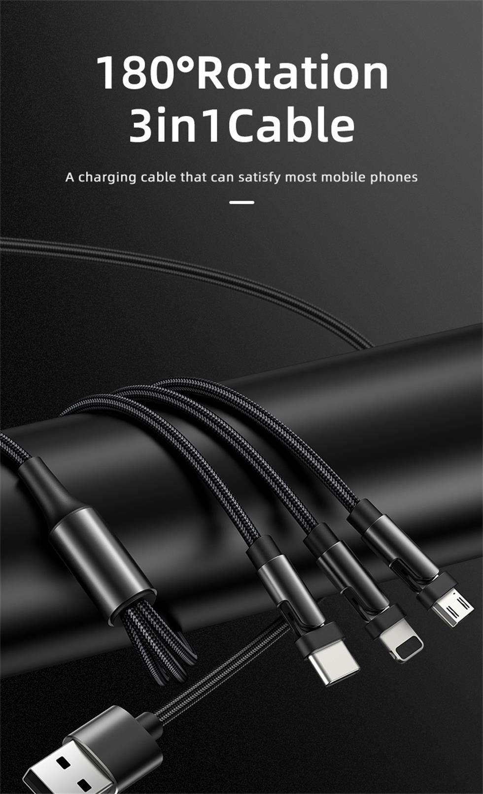
Nowadays, the function and appearance of mobile phones are similar, but the charging interface is not unified. The Android camp has Micro USB and Type-C ports, while the iPhone camp has Lightning. Different charging ports use different charging cables, which is very unfriendly for users who often need to use multiple phones. To solve this awkward situation, the three-in-one data cable was born. What is the three-in-one data cable? Three-in-one data cable means that one data cable includes Micro Usb Cable, USB Cable For Iphone and Usb Cable Type C. So one data cable can be used by all mobile phones.
Three-in-one data line is also known as multifunctional data cable. In the original data cable, the combination scheme is added, and the combination PCB is configured, which can support a variety of equipment and avoid the trouble of frequently looking for data line. It combines Lightning, a 30-pin port, and a Micro USB port, and is compatible with multiple devices. It can connect to any smartphone or tablet, including iPhone, iPad, Samsung, etc.
From the technical point of view, the three-in-one data cable does have a strong advantage. With continuous development and improvement, three in one data cable products in the original data cable appearance with woven cloth, will also add a light color on the three in one data cable, so that the data cable function is stronger and more exquisite, more and more people accept and buy. In the era of big data,the 3 In 1 Usb Cable can be said to have deeply affected our work and life. We believe that with the technical development of 3-in-1 mobile phone data cable, it will bring us more convenient transmission experience.
3 In 1 Usb Cable,3 In 1 Data Cable,3 In 1 Usb C Cable,3 In 1 Universal Cable
Henan Yijiao Trading Co., Ltd , https://www.yjusbhubs.com
