DDR wiring in PCB design applications, what do you think?
DDR cabling plays a pivotal role in PCB design. The key to successful design is to ensure that the system has sufficient timing margin. To ensure the timing of the system, line length matching is an important part.
Let's review, DDR routing, the basic principle of line length matching is: address, control / command signal and clock are equal. The data signal is equal in length to the DQS. Why do you have to wait for the same length? You will say that the same group of signals should arrive at the receiving end at the same time, so that the receiving chip can process these signals at the same time. Then, the clock signal and the address arrive at the receiving end at the same time, what is the corresponding relationship of the waveform? We look at the specific waveform through simulation. Establish the following channels to simulate the address signal and clock signal of DDR3.

Figure 1 Address / clock simulation diagram
For the convenience of calculation, we assume that the clock frequency of DDR is 500MHz, so the corresponding address signal rate should be 500Mbps. Here we should understand that although DDR is double rate, it is still single speed for address/control signal. Rate. Let's take a look at the waveform. When the address and the clock are exactly the same length, the receiving waveform of the address and data is as shown in Figure 2. Red represents the address signal and green represents the clock signal.
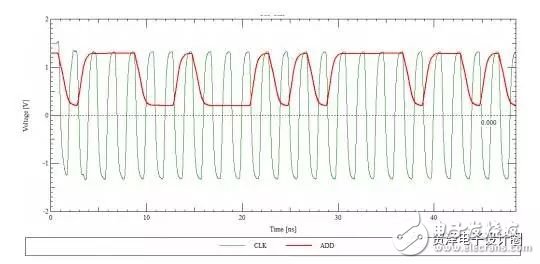
Figure 2 Clock signal and address signal waveform
The waveform above does not seem to see what the timing relationship between the clock and the address is. We put it in an eye diagram and the timing relationship is clear. Here is a rough calculation of the setup time and hold time. As shown below

Figure 3 Clock signal and address signal waveform
From the above figure 3. We can know that the setup time of this address signal is about 891ps and the hold time is 881ps. This is the waveform when the clock and address signals are exactly equal. If the address is not equal to the clock, what is the signal? In the simulation, we make the address line 200 ps slower than the clock line. The resulting eye diagram is as follows:

Figure 4 Clock signal and address signal waveform
As can be seen from the above figure, in the case where the address signal is longer than the clock signal, the hold time is 684 ps, and the setup is 1.1 ns. It can be seen that the address line is longer than the clock line with respect to the length of the address line and the clock line, so that the setup time of the address signal is shorter. Similarly, if the clock line is longer than the address line, the settling time will be longer and the hold time will be shorter. So what is the double-rate data signal? Let's look at the specific simulation example below.

Figure 5 DQ and DQS simulation
The simulation channel is shown in the figure above. The driver and receiver are the IBIS models of a chip company. The simulation waveforms are as follows:
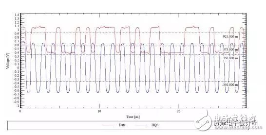
Figure 6 DQ and DQS simulation waveforms
We generate the eye diagrams simultaneously with the DQS and DQ signals, and observe them in a window. The results are as follows:

Figure 7 DQ and DQS eye diagram
As shown in the figure above, you may find that if the original signal is used, the edge of the data signal and the edge of the clock signal are aligned. If so, how does the clock signal complete the sampling of the data signal? Actually, this is not the case. . The above simulation simply puts the two waveforms together, because the transmission channels of DQ and DQS are the same length, so their edges are aligned. In actual work, the main control chip will have an adjustment mechanism. The general data signal will be released a quarter of a cycle earlier than the DQS. In fact, the waveform correspondence received at the particle end should be like this:
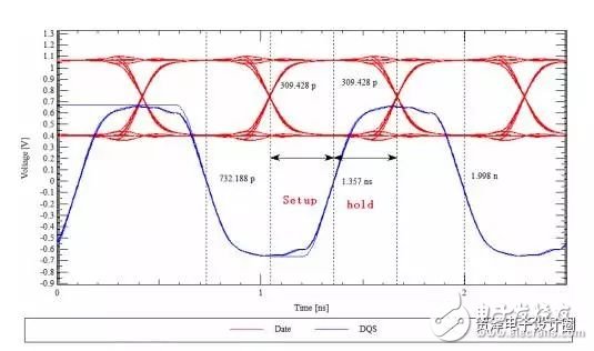
Figure 8 Eye diagram after translation
After the adjustment of the master chip, the edge of the DQS is aligned with the center of the DQ signal bit, thus ensuring sufficient setup and hold time for the data to be transmitted to the receiver. As with the above analysis of the clock and address signals, if the equal length between DQ and DQS is not good, the clock edge of DQS will not remain in the middle of DQ, so the margin of setup time or hold time will become smaller. Let’s take a simple look at a picture
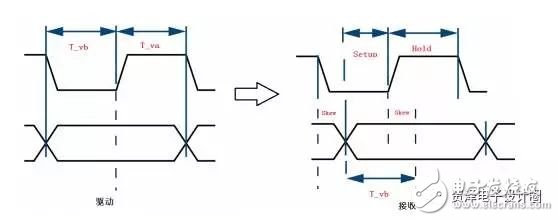
Figure 9 Effect of delay deviation on timing
In the above figure, T_vb and T_va represent the timing parameters between the clock and the data when the master chip outputs data. Ideally, the center of the clock and the center of the data level are aligned. Since the clock and data transfer channels are not of equal length, the clock edges are not centered with the data pulses, making the settling time margin smaller. After understanding these basic questions, all we need to do is convert these time parameters into line lengths.
Below we take a concrete example to look at the timing calculation. The following figure is the Freescale MPC8572 DDR master chip manual. This picture defines the phase relationship between DQS and DQ when coming out of the chip.
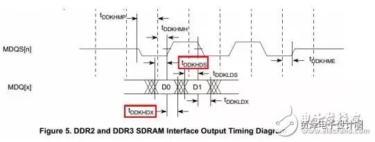
Figure 10 MPC8572 timing diagram
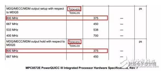
Figure 11 MPC8572 timing parameters
The particle end is Micron DDR. The timing diagram and timing parameters of the chip are shown in the figure below. This picture defines the setup time and hold time required for the chip end chip identification signal.
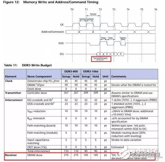
Figure 12 DDR particle timing diagram and timing parameters
We use T_pcbskew to represent the delay skew between DQ and DQS. If you want to get enough timing margin, the delay bias should satisfy the following relationship:
T_pcbskew "T_vb-T_setup T_pcbskew" T_hold-T_va substitute data, there are: T_vb-T_setup=375-215=160ps T_hold-T_va=-160ps
Thus, if the speed of the transmission line is calculated at 6 mil/ps, T_pcbskew is +/- 960 mil. You will find that the margin is very large. Of course, this is only the ideal situation. It does not consider the jitter of the clock and the jitter of the data signal, as well as the impact of crosstalk and intersymbol interference. If these factors are taken into account, leave us with the wiring deviation. The margin is relatively small. In summary, the purpose of timing control is to ensure that the data has sufficient setup time and hold time at the receiving end. Understand this point, we can achieve a confident and straightforward online matching problem.
Blank Shirts,Black Long Sleeve,Short Sleeve Hoodie,Woolen Sweater For Women
GUANGZHOU LIWEI ELECTRONICS CO.,LTD , https://www.gdliwei.com
