Design of 1024-point Digital Pulse Compression System Using FPGA of ADS5500
The pulse compression system is widely used in modern radars. By transmitting wide pulses, the average power of the transmission is increased to ensure sufficient range; when receiving, the corresponding pulse compression algorithm is used to obtain pulses with a narrow pulse width to improve the range resolution. , Which can well solve the contradiction between the range of action and the distance resolution.
The linear frequency modulation (LFM) signal expands the signal bandwidth by adding a carrier linear modulation in a wide pulse to obtain a larger compression ratio. The required matched filter is not sensitive to the Doppler shift of the echo signal, so the LMF signal is still widely used in many radar systems.
Based on the reusable and reconfigurable features of the Fast Fourier IP core, this paper implements a frequency domain FPGA digital pulse compression processor, which can complete the pulse compression of the variable-point LFM signal with orthogonal input, which is flexible in design and easy to debug. , Features of strong scalability.
1 System function hardware realization methodThis system is the data acquisition and digital pulse compression part of a broadband radar system. The system requires that the data acquisition of the distance channel and the digital pulse compression of 1,024 points be completed within 1 pulse repetition period (PRT), and the pulse pressure result is transmitted to the DSP in the current PRT. The hardware structure is shown in Figure 1.
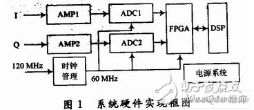
The data acquisition system mainly includes front-end operational amplifier and analog/digital converter. The operational amplifier selects AD8138 of ADI Company, converts the input signal from single-ended to the differential form to meet the input demand of ADC, and eliminate the influence of common mode noise. The analog/digital converter uses TI's ADS5500, which has a resolution of 14 b and a maximum sampling rate of 125 MSPS, and is used to sample the input LFM signal at a high speed of 60 MHz.
The digital pulse compression module is realized in FPGA, and FPGA chooses XQ2V1000 chip of Xilinx Company. After the input sampling data is pulse compressed, the result is stored in the dual-port RAM on the FPGA chip, and an interrupt signal is sent to the DSP. DSP reads the pulse pressure data in RAM for main processing after receiving the interrupt signal.
2 Design and realization of pulse compression module 2.1 Principle of pulse compressionDigital pulse compression technology is a practical application of matched filtering and related receiving theories. Matched filtering in the frequency domain is equivalent to related reception in the time domain. Figure 2 shows the principle of digital pulse compression based on matched filtering theory.

In Fig. 2 θ(f) is the non-linear phase spectrum of the transmitted signal, and the non-linear phase spectrum of the received echo signal is corrected after matched filtering. The narrow pulse output is:

The matched filter has an important characteristic: it is adaptable to signals with the same waveform but different amplitudes and delays. In other words, the filter matched to the signal s(t) is also matched to the signal as(t-Ï„). The position of the echo signal s(t) in the wave gate reflects the position where the peak of the pulse pressure result appears, which is also the main basis for the use of radar pulses for ranging.
2.2 Principle of pulse compressionThe pulse compression module includes FFT, and IFFT unit, complex multiplication unit and storage unit, and its structure block diagram is shown in Figure 3. Among them, the FFT and IFFT units are realized by multiplexing the fast Fourier transform IP core provided by Xilinx, and the hardware multiplier provides a solution for complex multiplication.
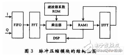
The sampled data is first stored in the FIFO for global buffering, and then the FFT unit reads the sampled data from the FIFO, and then performs the FFT operation. The result is directly multiplied by the matched filter coefficient during the pipeline output, and the operation result is written into the block RAM1 Finally, the IFFT unit reads the multiplexed data from the block RAM1 and performs IFFT (multiplexed FFT operation IP core) operations, and sends the interrupt signal after the result is written into the block RAM1, waiting for the DSP to read.
2.2.1 Hardware multiplexing of FFT processing unitThe FFT processing unit in the system uses the soft-core Fast Fourier Transform. v3. O to achieve. The IP core provides 3 structural options.
(1) Pipeline level, data pipeline I/0. This structure cascades several base-2 butterfly units so that data input, calculation, and output can be performed in a pipeline, which can achieve a high processing speed, but consumes a lot of resources;
(2) Base-2, the least resource consumption. This structure uses a single base-2 butterfly unit to transform the input data, and the operation consumes a long time;
(3) Base-4, burst I/O; this structure uses a single base-4 butterfly unit to transform the input data, and uses block RAM to store the twiddle factor, which occupies less system resources, in 1 PRT It can complete the output of pulse pressure results, so as to achieve a good balance between resources and speed, which is also the structure actually adopted in the design.
The FFT processing unit mainly includes two processes: data I/O and arithmetic process, but the two are not executed in a pipeline. After the FFT start signal is valid, the data starts to load, and the FFT operation starts after the load is completed; the result can be output after the operation is over. During the operation, no data loading or output occurs.
In digital design, FFT and IFFT processing units can be implemented with the same structure. The specific method is: before doing the IFFT operation, first exchange the real and imaginary parts of the input data, and then send it to the FFT processing unit to perform operations according to the FFT structure, and exchange the real and imaginary parts of the FFT operation result, and finally divide by The number of operation points N, you can get the result of the IFFT operation.
Based on the above method, the IP core also has the function of performing IFFT operations. By configuring the level on the port FWD INV in real time, multiplexing can be achieved, and FFT and IFFT operations can be completed respectively. In FPGA design, the use of structure multiplexing to reduce logic unit blocks can not only save system resources, but also reduce hard wiring and transmission line delays between structures, which is beneficial to increase the operating frequency of the system.
2.2.2 Timing design of pulse compression moduleBecause the logic operation functions of FFT and IFFT have been implemented in the IP core, the timing design is particularly important. In the FFT (or IFFT) arithmetic unit, the main state and timing control signals and their function descriptions are shown in Table 1.
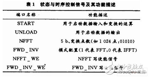
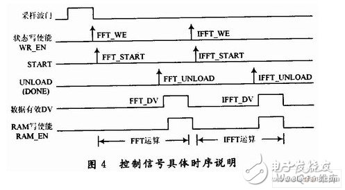
During the valid period of the sampling distance gate, the sample data is written into the FIFO for buffering. After sampling, through the write enable signal (NFFT_WE and FWD_INV_WE) of the FFT unit, write NFFT=010 10 and FWD_INV_WE=1 to the status control register to set the working mode, and then start the START signal for FFT operation, write enable signal and sTART There is only 1 clock cycle difference between. After the operation, the DONE signal is valid for 1 clock cycle, and the output enable signal UNLOAD is synchronized with DONE. After 7 clock cycles, the data valid signal DV becomes valid, and the FFT operation result starts to be output in a pipeline, and it is multiplied by the matched filter coefficient. , And store it in RAM. Due to the inherent delay of the multiplication operation, the write enable RAM_EN delays the DV signal by 2 clock cycles. At the end of storage, the write enable signal of the IFFT unit is valid at the same time, and NFFT=01010 and FWD_INV_WE=0 are set, and then the START signal is started for IFFT operation. After the operation is over, the DONE signal (synchronized with UNLOAD) is valid again, and the output result of the IFFT operation is directly written into the RAM during the valid period of the DV signal. The specific timing description of each control signal in a single PRT is shown in Figure 4.
In the digital signal processing system, the data representation format can be divided into fixed-point system, floating-point system and block-floating-point system. They have different requirements for system resources and different working speeds when they are implemented, and they have different scopes of application. The fixed-point representation is the most used, simple and fast, but the dynamic range is limited. It is necessary to appropriately compress the dynamic range of the input signal with appropriate overflow control rules (such as the fixed ratio method), but this will reduce the signal-to-noise ratio of the output signal. The advantage of floating-point representation is that it has a large dynamic range, can avoid overflow, and can achieve a high signal-to-noise ratio in a large dynamic range. The main disadvantages are complex system implementation, large hardware requirements, high cost and power consumption, and The speed is slower.
Block floating-point representation has some advantages of fixed-point and floating-point, and is a combination of the above two representations. This notation first detects a set of data, normalizes the decimal part of the largest number, and then establishes an appropriate exponent. Then convert the fractional part of the remaining data into appropriate numbers so that they can use the largest number of exponents. The main advantages of the block floating-point algorithm are: large dynamic range, low truncation (or rounding) noise, and it is an effective form of data representation. From the point of view of chip implementation, the block floating-point representation can guarantee higher signal processing quality, and is especially suitable for FFT operations. The FFT core in the pulse compression module has the function of block floating point operation, and the data format in the whole operation process is shown in Figure 5.
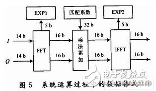
The ADC input data is in the form of twos complement of 14 b, and its low-order zero padding is expanded to 16 b (input accuracy required by the IP core) and then sent to the FFT operation unit. The output result is a fixed-point number of 16 b and exponent EXP1. Complex multiplication includes multiplication and accumulation, that is, the FFT result and the matching coefficient are multiplied by 16 b×16 b, and the result is then added; before the addition, all data is expanded to 33 b to prevent overflow, and finally The data is intercepted at a height of 16 b and sent to the IFFT processing unit. The output is a fixed-point number of 16 b and the exponent EXP2, which is added to EXP1 to obtain the exponent EXP. The final result of pulse pressure is the 16 b fixed-point number and exponent EXP after IFFT, which are stored in FPGA on-chip RAM respectively.
2.3 Test of pulse compression moduleSuppose the input ideal LFM signal parameters are as follows: bandwidth B=40 MHz; time width T=6μs; system sample rate is 60 MHz; use Hamming window weighting. Under the above conditions, the logarithmic diagram of the output result of the pulse compression system is shown in Figure 6.
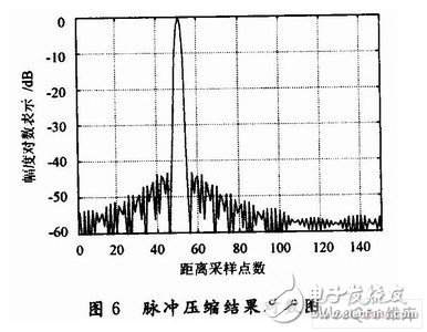
In Figure 6, the horizontal axis represents the distance sampling unit, that is, the minimum distance resolution of the system. The correctness and practicability of the design are verified by comparing the actual processing results of the system and the Madab simulation results.
3 ConclusionThe system uses ADS5500 to complete 14-bit, 60 MSPS data acquisition, and implements 1,024-point digital pulse compression in FPGA. The design adopts the parallel pipeline method to improve the working speed, and the block floating-point algorithm fully guarantees the accuracy of the operation. The multiplexing of the IP core greatly reduces the hardware scale, so that the entire system has the characteristics of high speed, high precision and low power consumption.
Disposable Vape,Disposable Vape Pen,Disposable Vape Elf Bar Lux,Disposable Vape Pod Device
Shenzhen Zpal Technology Co.,Ltd , https://www.zpalvapes.com
