Design of transmitting platform of pseudorandom code phase modulation radar based on AD9857
Design of transmitting platform of pseudorandom code phase modulation radar based on AD9857
High-frequency ground wave radar is used for continuous large-area marine environment monitoring, which can detect sea surface dynamic parameters such as wind, waves, currents and tides in real time. Its research and development are of great significance to offshore operations, marine development and national defense [1].
The rapid development of programmable logic devices in recent years has promoted the development of software radio technology. Due to the lack of flexibility of traditional radar transmitting and receiving systems based on discrete devices, and various parameters are not easy to change, the new generation of high-frequency ground wave radar system will use a general hardware platform for transmitting and receiving based on the idea of ​​software radio to achieve radar operating parameters Programmability, thus enabling detection of different uses. And the entire radar system will be considered to further improve the integration, more and more modules will be designed based on the idea of ​​software radio. Compared with the frequency modulation interrupted continuous wave (FMICW) system adopted by the previous generation high frequency ground wave radar system, the new generation radar system uses the m series pseudo-random code phase modulation system and is based on the AD9857 digital quadrature upconverter and VXI bus transmission mode. This article will focus on the design of the m series pseudo-random code phase modulation module in the hardware platform of the new generation radar system.
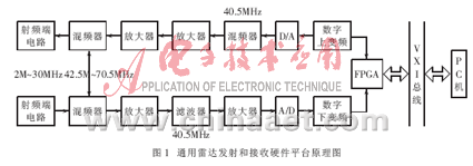
1 General radar transmitting and receiving hardware platform principle According to the requirements of radar parameters such as ranging accuracy and range resolution developed by our laboratory for high-frequency ground wave radar, a new generation of high-frequency ground wave radar system uses 40.5MHz processing intermediate frequency, radio frequency The signal frequency is 2M ~ 30MHz, and the receiver's LO frequency is 42.5M ~ 70.5MHz. Its block diagram is shown in Figure 1.

Radar launching process: Programmable logic device (FPGA / CPLD, the same below) is programmed to generate an m series of pseudo-random code phase modulation pulse signal, which is upconverted to 40.5MHz by AD9857 digital quadrature upconverter, after filtering and power The RF signal is obtained after amplification and mixing, and then amplified by the RF side circuit and power, and then fed to the antenna for transmission. Radar receiving process: the echo signal received by the antenna is filtered and amplified by the RF terminal circuit, mixed with the local oscillator signal to obtain an intermediate frequency signal, and then filtered and amplified and converted into a digital downconverter after the analog-to-digital conversion is processed for speed reduction The low-speed digital baseband signal is finally sent to the programmable logic device for related processing. At the same time, the signal processed by the programmable logic device is sent to the host PC via the VXI (VME Extension for InstrumentaTIon) bus. The biggest advantage of this design is that the transmitted pulse coded signal is generated by the programmable logic device, and the modification is flexible, and the processing of the received echo signal and the interface circuit with the VXI bus can be designed together in the programmable logic device, greatly The integration of the system is improved, which fully reflects the advantages of the software radio idea.
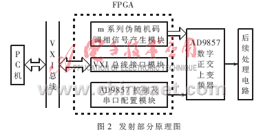
2 Design of the radar transmission part According to the above-mentioned radar transmission principle, the design method of the radar transmission part of the pseudo-random code phase modulation system based on the AD9857 digital quadrature up-converter is: the whole design uses Altera's FLEX10K series chips, developed at MAX + PLUSII Under the environment. The design of FLEX10K series programmable logic device mainly includes: m series pseudo-random code phase modulation signal series generation module, AD9857 control and serial port register configuration module, VXI bus interface module three parts. The design of the three modules is the focus and difficulty of the design of the entire launch part, and it is also the key technology. The design adopts the design method of the combination of hardware programming language VHDL text input and schematic input. The schematic diagram of the transmitting part is shown in Figure 2.

2.1 Design of each module in FPGA
2.1.1 Design of m series pseudo-random code phase modulation module In a common single-frequency pulse radar system, a single pulse with a width of? And a period of T is used to perform amplitude control on a sine or cosine carrier with a frequency of f0 to obtain pulse amplitude modulation wave. Although a simple pulse radar can obtain very high transceiver isolation and high range resolution, it has an obvious shortcoming that there is a contradiction between the range resolution and the actual maximum detection distance. Because if the distance resolution is very high, the width of the transmitted pulse is very small, the working ratio is very low, and the average transmitted power is also very low, resulting in a reduction in the actual detection distance [3]. On the contrary, if the maximum detection distance of the radar system is increased by increasing the pulse power, it will increase the difficulty of the transmitter and increase the failure rate.
In order to solve the above contradiction, pulse compression technology has been produced. Pulse compression technology is to make the radar system transmit a pulse with a relatively wide width and a low peak power. Using this technology can increase the maximum detection distance of the system without increasing the difficulty of the transmitter. Pulse compression technology is realized by spreading the carrier code in the transmitting part, and then compressing the echo in the receiver. Current pulse compression methods generally use two types of waveforms: linear frequency modulation interrupted continuous wave (FMICM) and pseudorandom code phase modulation interrupted continuous wave. A new generation of high-frequency ground wave radar systems will use pseudo-random code phase-modulated continuous waves.
In the pseudorandom code phase modulation system, m series pseudorandom codes are generally used. The m sequence is a very important pseudo-random sequence, which is widely used in radar systems and spread spectrum communications. Features of m series: (1) Random characteristics with random sequences (ie statistical characteristics). (2) is a determination sequence that can be determined in advance and can be repeatedly implemented. (3) It has very good autocorrelation characteristics. Its autocorrelation function has only two different values, that is, it has dual-value autocorrelation function characteristics. (4) The longest sequence that can be produced by linear shift registers with the same number of stages. This design uses m series pseudo-random codes.
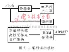
The m series pseudo-random code phase modulation module is mainly composed of the parts shown in FIG. 3. First, a frequency divider generates the m series generation frequency and the operating frequency of the phase modulator. The design of this part should consider the working principle of other parts. Because the address generation frequency of the sine and cosine sampling discrete point values ​​in the phase modulator should be 100 times the m series generation frequency, the frequency divider must first divide the clock 100 times, and the divided frequency is used as the m series Generate the clock frequency, and clock as the sine and cosine discrete sampling point value address generation frequency.

In the high-frequency ground wave radar system, 8 levels are initially adopted, that is, m series with 28-1 = 255 code lengths, and the length of each symbol is taken as Te = 64μs. Because there are many series, it is appropriate to use text input to generate the m series. According to the relationship between the characteristic polynomial coefficients of the m sequence and the feedback coefficients of the m sequence generator, a variety of coefficients can be formed: c0 = c4 = c5 = c6 = c8 = 1, c1 = c2 = c3 = c7 = 0 ] 'S 8-level m-sequence generator.
Binary phase modulation means that when the symbol of the digital baseband signal is 0, the carrier phase takes π to invert the output waveform; when the symbol of the baseband signal is 1, the carrier phase takes 0, and the output waveform is unchanged. In this way, the corresponding baseband pulse information is expressed in different phases of the carrier, and the frequency expansion is achieved [5]. The carrier signal in this design is a series of sine and cosine discrete sampling point values. Through experiments, it is found that in each m-series baseband symbol time period, that is, within 64 μs of this design, 100 points of carrier sampling can better meet the design requirements. The generation of carrier discrete sampling point values, that is, the design of sine and cosine discrete sampling point value blocks, should consider the data format and data input rate requirements of the parallel data input terminal of the AD9857 digital quadrature upconverter. Here AD9857 chip should produce I / Q 2-way orthogonal carrier discrete sampling point value and 14-bit complement format conversion of the data. Since there is no sine and cosine generating function in the VHDL hardware programming language, this design first uses C language to generate I / Q 2-channel sine and cosine discrete sampling point values, and converts to 14-bit complement format, and then converts 14-bit complement The point values ​​of the format are stored in a ROM block, and their value addresses are generated by the phase modulator. Altera's FLEX10K series chips are used in this design to contain embedded array blocks (EAB), which can be used to construct ROM memory.
The phase modulator part mainly generates the value address of the point value in the ROM memory, and completes the phase modulation function at the same time. When the m-sequence baseband symbol is 0, the carrier phase is inverted. According to the characteristics of the sine and cosine waveforms, the addressing point can be jumped to when the symbol jumps from 1 to 0 (jump-low = 1) At sinπ (that is, at the 51st point value), phase inversion can be achieved; when the m-sequence baseband symbol is 1, the carrier phase is unchanged, and the addressing point can jump from 0 to 1 (jump_high) = 1), return to sin0 (the first point value). Since 100 points of the sine discrete sampling point value are stored first in the ROM storage table, and then 100 points of the cosine discrete sampling point value are stored, the VHDL addressing program of this part can be designed as follows.
if (count202s = "01100100") and (jump_low = ′ 0 ′) then
-Sinusoidal discrete sampling point value part count202s <= "00000000";-Addressing to the 100th point value and-When it is not the next edge of the symbol, return to the 1st point value elsif (jump_high = ′ 1 ′) then count202s <= “00000000â€;
--When the symbol jumps up, it is addressed to the first point, and the modulation phase is 0
elsif (jump_low = ′ 1 ′) then count202s <= “00110010â€;
--When the symbol jumps down, it is addressed to the 51st point value, and the modulation phase is 180 °
else count202s <= count202s + ′ 1 ′;
end if;
if (reset = ′ 1 ′) then count202c <= “01100101â€;-Cosine Discrete--The sampling point value address value is initialized to the 101st point value elsif (en = ′ 1 ′) then
if (count202c = "11001001") and (jump_low = ′ 0 ′) then
count202c <= "01100101";-When addressing to the 200th point value and--not the next edge of the symbol, return to the 101st point value elsif (jump_high = ′ 1 ′) then count202c <= "01100101";
--When jumping up, address to the 101st point, the modulation phase is 0
elsif (jump_low = ′ 1 ′) then count202c <= “10010111â€;
--When the symbol jumps down, it is addressed to the 151st point, and the modulation phase is 180 °
else count202c <= count202c + ′ 1 ′;
end if;
end if;
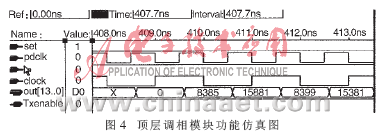
The compiled simulation waveforms of m series phase modulation modules are shown in Figure 4. It can be seen from Figure 4 that the function of this module is completely correct.

2.1.2 AD9857 control and serial port configuration module AD9857 digital orthogonal up-converter mainly has two parts: parallel port and serial port. The input data of the parallel port is provided in turn by the baseband data stream of the 14-bit complement format of the I / Q2 channel after the phase modulation of the m series pseudo-random codes. The configuration of each register in the serial port is the key to the entire design, including the setting of working mode, frequency control word, clock frequency multiplication, filter interpolation factor and output gain control. According to the serial port read and write timing requirements, the design of this part is implemented in VHDL language programming.
2.1.3 Design of VXI bus interface module VXI bus is a new type of instrument system bus developed on the basis of VME bus and GPIB bus. It draws on the advantages of the VME and GPIB buses, and combines the characteristics of the instrument measurement system to add many new features, such as zero-slot module functions, resource managers, power distribution, cooling, and electromagnetic compatibility [6]. The new generation of high-frequency ground wave radar system is based on the VXI bus transmission mode.
VXI bus module instrument can be divided into 4 parts: register base, message base, memory base and expansion device. The first two devices are used more. The basic requirement of the register-based device's VXI bus interface is that it only needs to have configuration registers, and the communication with this device is completed by reading and writing registers. It cannot control other devices and can only be controlled by other devices. The message-based device should not only have bus configuration registers, but also be able to perform more advanced communications and support more complex protocols, such as word-serial protocol, etc. It can control other devices and can also be controlled by other devices.
The signal transmission module in this design is based on a register base. In addition to the basic configuration registers in its VXI bus interface module, it is also compatible with other parts such as the receiving module due to the universality of the interface, so it also has an interrupt interface inside. , Data transmission interface, etc. The design of this part is also based on the VXI bus usage specifications and timing requirements, using the state machine in the VHDL programming language.
2.2 Digital up-conversion technology Traditional radar transmission systems generally use phase-locked loop (PLL) circuits to multiply the analog baseband signal to the carrier frequency required by the system, and then connect an analog multiplier to complete the modulation function. Compared with traditional phase-locked loop technology, digital up-conversion technology has the advantages of high frequency resolution, linear phase change, and easy digital control, etc. It is being used more and more widely. Typical digital upconverters are AD9856, AD9857 of AD company, HSP50215 of Harris company, and 4-way launch chip GC4114 of Gray company. This design uses AD9857. The AD9857 digital quadrature upconverter generally has three operating modes: quadrature modulation mode, single frequency output mode and interpolated DAC mode. When working in quadrature modulation mode, I / Q 2 digital baseband signals are alternately input, and then divided into 2 channels, which are sent to the quadrature modulator after passing through CIC filter and programmable interpolator. The DDS core provides a quadrature local oscillator signal to the quadrature modulator, multiplies and adds to the I / Q 2 channels of data, and generates a quadrature modulated data stream. These are all done in the digital domain. Finally, a quadrature-modulated analog signal is output through a 14-bit DAC; when working in single-frequency output mode, the AD9857 is equivalent to a DDS frequency source and does not accept external data. The DDS core generates a single-frequency digital signal under the control of the frequency control word, which is then output by the DAC; when working in the interpolated DAC mode, the 14-bit I channel data is input, and then output by the DAC after interpolation. In this mode, the signal is oversampled, but the original signal spectrum remains unchanged. In this design, quadrature modulation mode is used.
2.3 The follow-up processing circuit can be seen from Figure 2. The follow-up processing circuit mainly includes the A / D conversion, filtering and power amplification of the intermediate frequency analog signal after up-conversion by the AD9857 digital quadrature upconverter. The goal of software radio is to start digitizing the signal at a higher intermediate frequency or even the radio frequency section, which can reduce the number of analog devices in the system and increase the flexibility of the system. To meet this requirement, the ADC must have a high sampling rate and operating bandwidth. In order to adapt to the complex electromagnetic environment, ADC also requires a large dynamic range. At this time, the intermediate frequency output signal requires a high-frequency narrow-band filter for filtering. The general LC filter cannot meet the requirements. A quartz crystal resonator with a high operating frequency stability, a steep stopband attenuation characteristic, and a small insertion loss should be used. For the high-frequency narrow-band filter, the amplifier circuit should adopt a low-noise high-bandwidth adjustable gain amplifier. What is used in this design is the AD603, a low-noise adjustable gain amplifier with a bandwidth of 90 MHz.
3 Conclusion Based on the idea of ​​software radio, the intermediate frequency of a new generation of high-frequency ground wave radar system using m series pseudo-random code phase modulation system will reach 40.5MHz. Therefore, some key technologies must be breakthrough, mainly including digital up-conversion technology and digital down-conversion technology, high-speed A / D and D / A conversion technology, open bus structure technology and high-speed digital signal processing technology. The scheme of the high-frequency ground wave radar transmitting part system of the pseudo-random code phase modulation system based on the AD9857 digital quadrature up-converter in this design is implemented according to the above requirements, and has achieved initial success.
Fiber Optic Splice Closure,Fiber Optic Splice Case,Fiber Splice Closures,Outdoor Fiber Optic Splice Closure
Cixi Dani Plastic Products Co.,Ltd , https://www.cxdnplastic.com
