High-power LED packaging technology
The process design of the LED includes the design of the chip and the packaging of the chip. At present, the packaging technology of high-power LED and its heat dissipation technology are hotspots in today's society. Since the high-power LED packaging process is simpler to say, the actual process is very complicated. And LED packaging technology directly affects the life of the LED. Therefore, in the process of high-power LED packaging, many factors must be considered, such as light, heat, electricity, machinery and many other factors. Optical aspects should consider the high-power LED light decay problem, thermal considerations should consider the heat dissipation of high-power LEDs, electrical considerations should be taken into account the design of the drive power of high-power LEDs, mechanical considerations should be taken into account the packaging form of LEDs in the packaging process. Wait.
1 High power LED package requirements and key technologies
(High power) LEDs have the advantages of long life, low pollution, low power consumption, energy saving and impact resistance. Compared with traditional lighting fixtures, (high-power) LEDs not only have good monochromaticity, high optical efficiency, high light efficiency, but also can meet different needs of high color rendering index. Despite this, the packaging process for high-power LEDs has strict requirements.
Specifically: 1 low cost; 2 system efficiency maximization; 3 easy to replace and maintain; more than 4 LEDs can be modularized; 5 low heat dissipation coefficient and other simple requirements.
According to various factors to be considered in high-power LED packaging technology, several points have been proposed in the key technologies of packaging. mainly include:
(1) In terms of high-power LED heat dissipation: Consider a low thermal resistance package. The LED chip is a solid-state semiconductor device that is the core of the LED light source. Since the high-power LED chips are of different sizes, the driving method uses a constant current driving method. The electric energy can be directly converted into light energy. Therefore, the LED chip needs to absorb most of the input electric energy during the lighting process, and a large amount of heat is generated in the process. Therefore, the heat dissipation technology for high-power LED chips is an important technology for LED packaging technology, and also a key problem that must be solved in the process of high-power LED packaging.
(2) The heart of the LED is a semiconductor wafer. One end of the chip is attached to a bracket, one end is a negative pole, and the other end is connected to the positive pole of the power source. Therefore, the high light extraction package structure is also an important key technology in the high power LED packaging process. In the process of illuminating the LED chip, during the emission process, due to the difference in refractive index at the interface, the loss of photon reflection and the possible total reflection loss may be applied, so that a relatively high refractive index of the chip surface may be coated on the surface of the chip. glue.
This layer of transparent plastic must have high light transmittance, high refractive index, good fluidity, easy spraying, and good thermal stability. Currently commonly used transparent adhesive layers are epoxy resin and silica gel.
2 LED package form
With the development of science and technology, LEDs can be packaged in a variety of forms, including leaded packages, surface mount chip packages, chip-on-chip packages, and system package packages.
Low-power LED packages are typically packaged in a leaded LED package. Leaded LED packages are also common. Ordinary LEDs are basically in a lead package. The heat of the lead-type LED package is radiated from the lead frame of the negative electrode to the PCB board, and the heat dissipation problem is also better solved. However, there are certain disadvantages, that is, the thermal resistance is large, and the service life of the LED is short.
Surface Mount SMD Package (SMT) is a new type of LED package that encapsulates an already packaged LED device into a fixed location. The advantages of SMT packaging technology are high reliability, easy automation, and high frequency characteristics. The SMT LED package is one of the most popular chip package processes in the electronics industry today.
The chip-on-board (COB) LED package technology is a direct mount technology that is a process of directly attaching a chip to a printed circuit board, then stitching the leads, and finally protecting the chip and the lead using organic glue. The COB process is primarily used in high power LED arrays. Has a high degree of integration.
System-packaged (SIP) LED packaging technology is a technology that has been developed in recent years.
It mainly meets the requirements of system portable and system miniaturization. Compared to other LED packages, SIP packages are the most integrated and relatively low cost. Multiple LED chips can be assembled in one package.
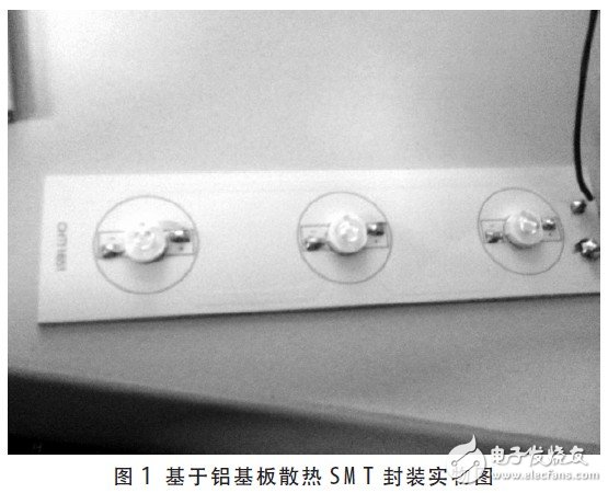
In the actual application process, according to the requirements of the experiment, the author uses the form of SMT package. In the high-power LED packaging process, taking into account the high-power LED heat dissipation factor, I use the traditional way of using aluminum substrate cooling. Through practical applications, we found that SMT packaging technology meets the actual thermal requirements. The concrete physical map of the physical aluminum substrate is shown in Figure 1.

New Energy Vehicle Parts & Accessories
Shenzhen Jiesai Electric Co.,Ltd , https://www.gootuenergy.com
