How difficult is chip manufacturing? The real chip manufacturing process is very complicated
The ZTE incident in April of this year aroused the public's attention to domestic chips. According to statistics, in 2017, domestic imports of integrated circuits were still as high as US$2601.4, and the import and export deficit reached US$193.2 billion. Obviously, China's current dependence on foreign chips is still very high.
How difficult is chip manufacturing?
Chip production is a process of turning sand into gold. From sand to wafer to chip, the value density has soared. The real chip manufacturing process is very complicated, let's briefly introduce it for you.
Wafer refers to the silicon wafer used in the production of silicon semiconductor integrated circuits. Because of its circular shape, it is called wafer. From wafer to chip alone, its value can be doubled by 12 times. After 2,000 yuan of wafer raw materials are processed, the finished product is worth about 25,000 yuan, and you can buy a high-performance computer.
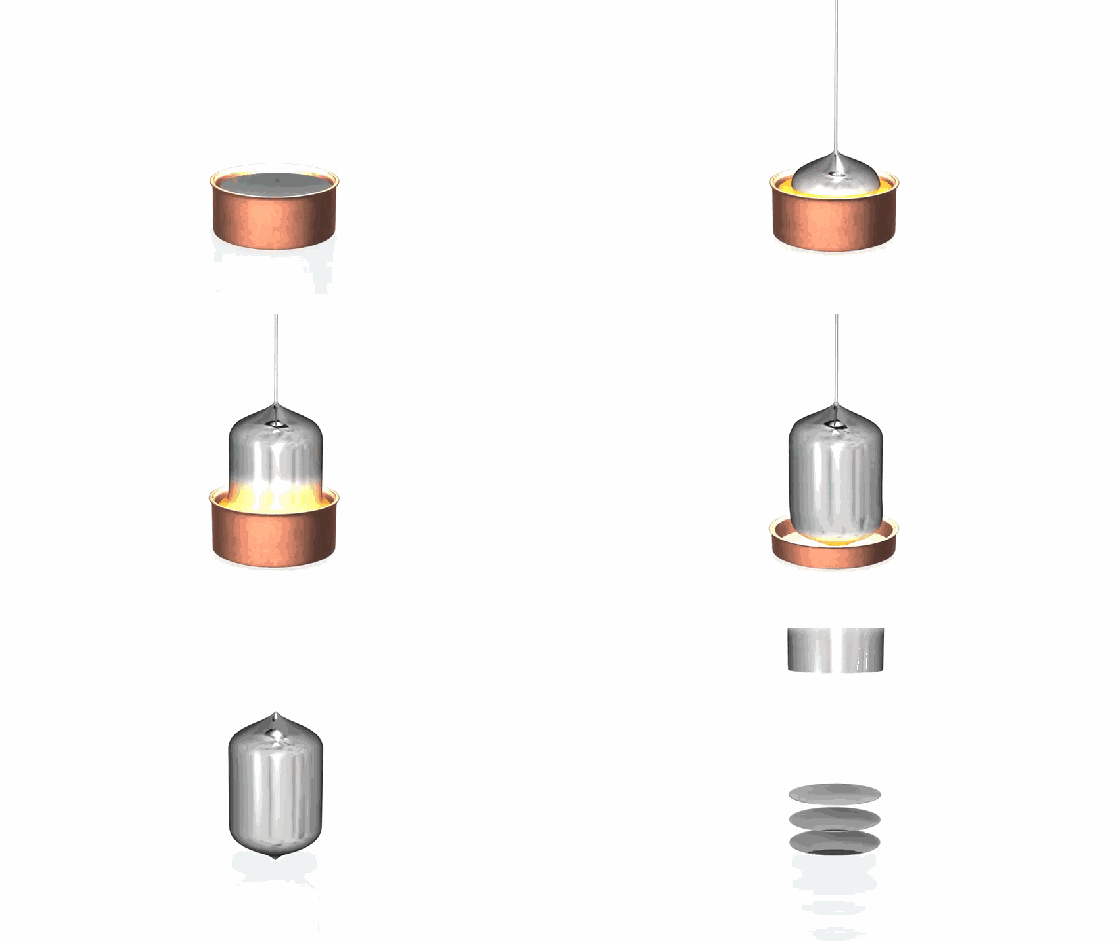
Pull out the wafer from the molten Si and slice it
After obtaining the wafer, apply the photosensitive material evenly on the wafer, and transfer the complex circuit structure to the photosensitive material using a photolithography machine. The exposed part will be dissolved and washed away by water, thereby exposing the surface of the wafer For complex circuit structures, an etching machine is used to etch away the exposed silicon wafers.
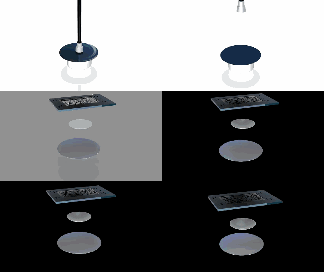
After the wafer is polished, the designed circuit is transferred to the wafer by a photolithography machine

Complex structures are etched on the wafer
Then, after hundreds of complex processes such as ion implantation, these complex structures have specific semiconductor characteristics, and hundreds of millions of transistors with specific functions can be manufactured within a range of a few square centimeters.
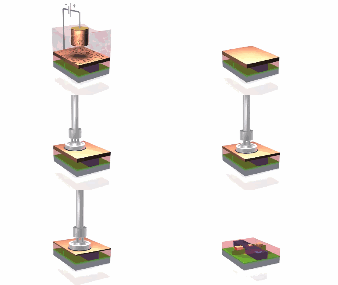
After copper plating, cut off the excess copper on the surface
By covering copper as wires, hundreds of millions of transistors can be connected.
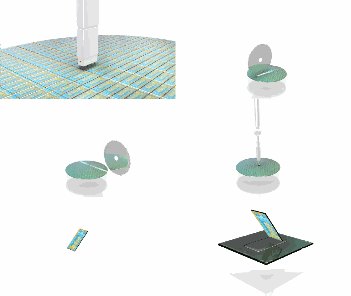
After testing, wafer dicing and packaging, we got the chips we saw
After several months of processing, a wafer integrates several kilometers of wires and hundreds of millions of transistor devices in a space the size of a fingernail. After testing, a qualified wafer will be cut, and the rest will be Scrapped. After thousands of choices, a real chip was born.
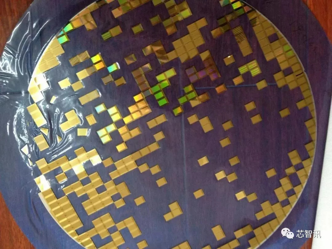
Wafers scrapped after cutting out qualified chips
Lithography machine-the card neck link of chip manufacturing
There are four major factors that restrict the development of integrated circuit technology: power consumption, process, cost and design complexity. Among them, the lithography machine is a top priority and the core of the core technology.
Some equipment has been dubbed "the jewel in the crown of industry" due to its huge manufacturing difficulty. The most mainstream argument is that there are two major equipment: aero engine and lithography machine. The most advanced aero engine is currently quoted in tens of millions of dollars. Class, but the current price of the most advanced lithography machine has exceeded 100 million U.S. dollars.
The degree of integration of the chip depends on the accuracy of the lithography machine. The lithography machine needs to achieve an image resolution of tens of nanometers or even higher. The two core systems of the lithography machine-the higher the accuracy of the optical system and the alignment system, can be The smaller the grooves carved on the silicon wafer, the higher the integration of the chip and the stronger the computing power.
At present, 80% of the world's lithography machine market is occupied by the Dutch company ASML, and EUV lithography machines capable of 7nm or even 5nm production are currently only available in the world by ASML. Coupled with the high cost of ASML's EUV lithography machine (ASML's highest-end EUV lithography machine NXE 3400B sells for about 120 million US dollars), and the production capacity is very limited, it can be said that a machine is difficult to find.
As mentioned earlier, Intel, TSMC, and Samsung all funded ASML around 2012 and became shareholders of ASML. ASML received a total of 1.38 billion euros (1.722 billion U.S. dollars) in research and development funds, which just reached the initial expected value, and 3.879 billion euros (4.839 billion U.S. dollars) were exchanged for a total of 5.259 billion euros (65.61 billion) through the transfer of 23% of the equity. One hundred million U.S. dollars). One of the reasons why Intel, TSMC, and Samsung chose to fund and invest in ASML is to promote the research and development of their EUV lithography machines and control the supply.
It should also be noted that due to the existence of the "Wassenaar Agreement", mainland China will be restricted from importing internationally advanced semiconductor equipment.
The "Wassenaar Agreement" is also known as the Wassenaar Arrangement Mechanism. It currently has 40 member states including the United States, Japan, the United Kingdom, and Russia. Although the "Wassenaar Arrangement" requires member states to decide on their own whether to issue export licenses for sensitive products and technologies, and to notify other member states of the "arrangement" of relevant information on a voluntary basis. But the "arrangement" is actually completely controlled by the United States. Mainland China is among the "embargoed" countries.
When the "Wassenaar Arrangement" a certain country intends to export a certain high technology to China, the United States even intervenes directly. For example, when the Czech Republic intends to export "passive radar equipment" to China, the United States put pressure on the Czech Republic to force the Czech Republic to stop. This transaction.
In fact, the embargo in the field of Chinese semiconductors has always existed. Intel, Samsung, and TSMC can buy 10nm lithography machines from ASML in 2015, while SMIC in mainland China can only buy ASML produced in 2010 in 2015. The 32nm lithography machine is enough for semiconductors in 5 years to update the market three times.
Although ASML has denied that it will be affected by the "Wassenaar Agreement" and SMIC has successfully ordered an EUV lithography machine this year, it will not be delivered until early 2019 at the earliest. That is to say, by 2019, SMIC can use EUV lithography machine to carry out some experimental research and development.
According to the current progress of SMIC, I am afraid that mass production of 10nm may not be possible until the end of 2020 at the earliest, but EUV is actually needed for the more advanced 7nm. Moreover, an EUV lithography machine can only be used for trial production at best, and it cannot be mass produced at all. Obviously, if SMIC wants to use EUV for mass production of 7nm, it needs to purchase more EUV lithography machines, and you don’t know how many ASML can sell in the future. It's almost 2022. By then, TSMC and Samsung's 3nm may all come out! The semiconductor manufacturing process in mainland China and overseas will still maintain a gap of the past two generations.
Of course, China also has its own lithography machine industry, but due to its late start and weak technology accumulation, the gap with foreign countries is still very huge.
As a leading domestic lithography equipment company, Shanghai Microelectronics Equipment (SMEE) currently can only provide up to 90mn process technology with the most advanced lithography equipment. In terms of indicators, it is basically at the same level as ASML's low-end product PAS5500 series. In addition, Hefei Xinshuo Semiconductor, Wuxi Yingsu Semiconductor and other companies can only provide up to 200mn process technology.
However, we do not have to be too pessimistic. At present, the country is also making key breakthroughs in the field of lithography machines. Among China's 16 major projects, the 02 project proposes that the lithography machine will be developed to 22nm by 2020. In 2015, 45nm and 65nm were industrialized. 45nm is the current mainstream lithography process, including 32nm and 28nm are basically improved and upgraded on the 45nm intrusion deep ultraviolet lithography machine. Therefore, it is very important for China to master 45nm. The 45nm lithography machine is a very important step. After reaching this level, the objective lens and polarization upgrade on the 45nm lithography machine can reach 32nm.
In addition, solid-state deep-ultraviolet light sources for lithography machines are also being developed. my country’s lithography machines are being developed in parallel, and the technology used in 22nm lithography machines is also being developed for 45nm upgrades. There are also electron beam direct writing lithography machines, nano-imprint equipment, and extreme ultraviolet lithography machine technologies are also being developed. Upgrade the photoresist, upgrade the refracting fluid, and use the over-etching method to reach the level of 22nm to 14nm or even 10nm. Corresponding upgraded photoresists, third-generation refractive fluids, etc. are also under development.
In terms of the most advanced EUV technology, last year's "Extremely Large Scale Integrated Circuit Manufacturing Equipment and Complete Processes" national science and technology major project "Extreme Ultraviolet Lithography Key Technology Research" successfully passed the acceptance. After eight years of hard work, the project research team has broken through core unit technologies such as ultra-high precision aspheric processing and testing, extreme ultraviolet multilayer film, and integrated testing of projection objective lens systems that restrict the development of extreme ultraviolet lithography in my country, and successfully developed wave imaging A two-lens EUV lithography objective lens system with a difference of better than 0.75nm RMS has constructed an EUV lithography exposure device, and obtained EUV projection lithography 32nm linewidth photoresist exposure pattern for the first time in China.
Of course, there is still a long way to go from technological breakthroughs to real commercial use to mass production. However, if we do not want to be stuck, we must dare to chew on this hard bone.
Automotive Connector 27P External Thread Assembly
Automotive Connector 27P External Thread Assembly
Automotive Connector 27P External Thread Assembly
ShenZhen Antenk Electronics Co,Ltd , https://www.antenkconn.com
