LTC3786 high efficiency synchronous boost power supply circuit
Below is the circuit diagram of the LTC3786 high efficiency synchronous boost power supply circuit.
The LTC3786 is a 98% high-efficiency synchronous boost power controller that does not require a heat sink. The VIN input voltage ranges from 4.5V to 38V, and the operating voltage is as low as 2.5V after startup. The output voltage is as high as 60V and the reference voltage is 1.2V±1%. Used for synchronous MOSFETs with 100% duty cycle capability. Static current 55uA, mainly used in industrial and automotive power supplies, automotive start systems, medical equipment and high voltage battery-powered systems.
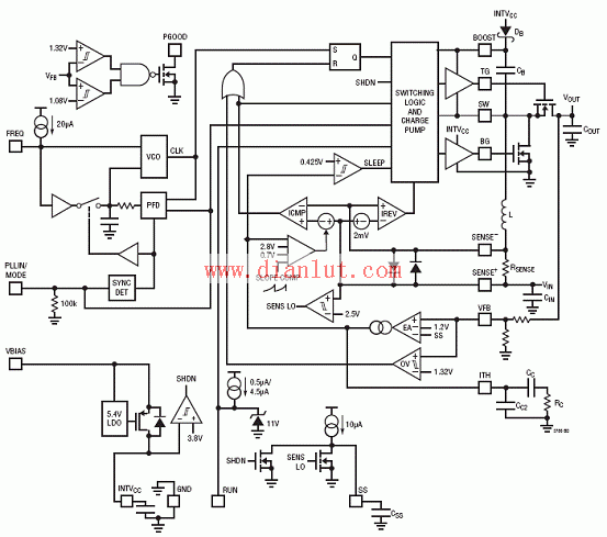
Figure 1. Block diagram of the LTC3786
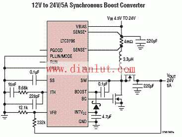
Figure 2. LTC3786 12V-24V/5A Synchronous Boost Converter Circuit
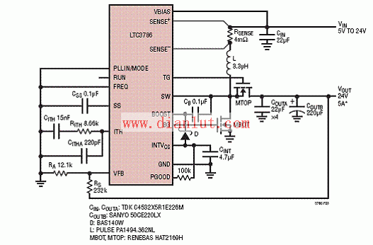
Figure 3. LTC3786 High Efficiency 24V Boost Converter Circuit
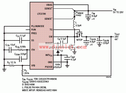
Figure 4. LTC3786 High Efficiency 28V Boost Converter Circuit
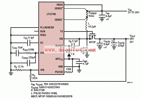
Figure 5. LTC3786 High Efficiency 36V Boost Converter Circuit
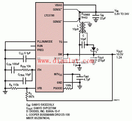
Figure 6. LTC3786 High Efficiency 10.5V Non-Synchronous SEPIC Converter Circuit
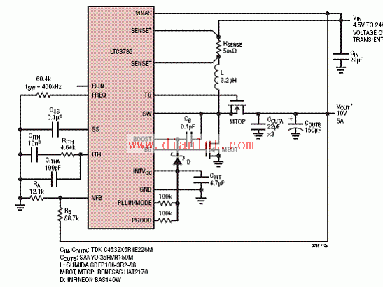
Figure 7. LTC3786 High Efficiency 10V Boost Converter Circuit
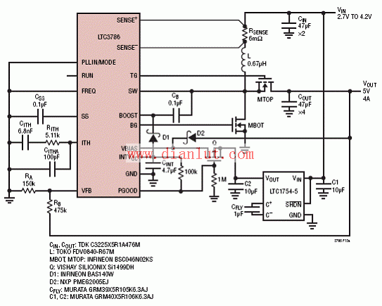
Figure 8. LTC3786 Low IQ Li-Ion 5V/4A Boost Converter Circuit
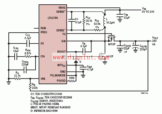
Figure 9. LTC3786 high efficiency 24V boost converter circuit with inductive DCR current sensing
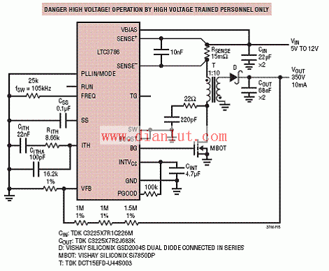
Figure 10. LTC3786 low IQ high voltage flyback power supply circuit
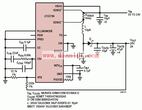
Figure 11. LTC3786 Low IQ Non-Synchronous 24V/2A Boost Converter Circuit
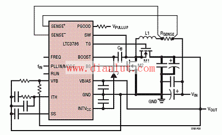
Figure 12. LTC3786 Recommended PCB Layout
Wired Headphone,Wired Gaming Headphones,Wired In Ear Headphones,Wired Bluetooth Headphones
Guangzhou YISON Electron Technology Co., Limited , https://www.yisonearphone.com
