Open-drain output and push-pull output
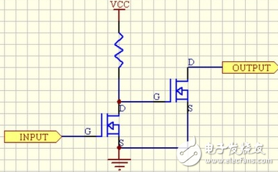
The open-drain (OD) output is very similar to the open-collector output. Replace the above triode with a FET. Thus the collector becomes the drain and OC becomes the OD. The principle analysis is the same. For an open drain (OD), the output corresponds to the collector of the transistor. A pull-up resistor is required to get a high state. It is suitable for current-type driving, and its ability to absorb current is relatively strong (generally within 20ma).
To achieve "wire and", an OC (open collector) gate is required. It is a triode or MOSFET with the same parameters and is present in the circuit in a push-pull manner. Each is responsible for the waveform amplification task of positive and negative half cycles. When the circuit is working, two symmetrical power switches have only one conduction at a time, so the conduction loss is small and the efficiency is high. The output can sink current to the load as well as current from the load.
We often encounter the concept of open drain and open collector in circuit design.
The "drain" mentioned in the concept of the open drain circuit refers to the drain of the MOSFET. Similarly, the "set" in the open circuit refers to the collector of the triode. An open drain circuit is a circuit that uses the drain of a MOSFET as an output. A common use is to add a pull-up resistor to the circuit outside the drain. The complete open drain circuit should consist of an open-drain device and an open-drain pull-up resistor. As shown in Figure 1:
The circuit that forms the open drain form has the following characteristics:
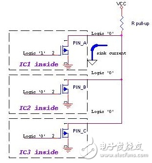
1. Reduce the drive inside the IC (or drive a load higher than the chip supply voltage) by using the drive capability of the external circuit. When the internal MOSFET of the IC is turned on, the drive current flows from the external VCC through R pull-up and the MOSFET to GND. Only a very low gate drive current is required inside the IC. Figure 1.
2. Pins of multiple open-drain outputs can be connected to one line. Form a "logical" relationship. As shown in Figure 1, when any of PIN_A, PIN_B, and PIN_C goes low, the logic on the open drain line is zero. This is also the principle that I2C, SMBus and other buses determine the bus occupancy status. If the output is connected, a pull-up resistor must be connected. When the capacitive load is connected, the falling delay is a transistor in the chip, which is an active driving, and the speed is fast; the rising delay is a passive external resistor, and the speed is slow. If the speed requirement is high, the power consumption will be large. Therefore, the choice of load resistor must balance power consumption and speed.
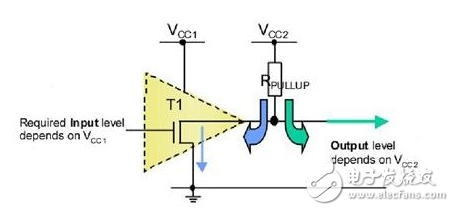
3. The transfer level can be changed by changing the voltage of the pull-up power supply. As shown in Figure 2, the logic level of the IC is determined by the power supply Vcc1, and the output high level is determined by Vcc2 (the supply voltage of the pull-up resistor). This way we can control the output high logic with low logic (so you can convert at any level). (For example, a pull-up resistor can be used to provide TTL/CMOS level output, etc.)
4. Open-drain Pin is not connected to the external pull-up resistor, it can only output low level (so for the classic 51 single-chip P0 port, to do the input and output function must add external pull-up resistor, otherwise it can not output high Level logic). In general, open drain is used to connect different levels of devices for matching levels.
5. Standard open drain feet generally have only the ability to output. Add other judgment circuits to have the ability to input and output in both directions.
6. The normal CMOS output stage is the upper and lower tubes. The removal of the tube above is OPEN-DRAIN. The main purpose of this output is two: level shifting, line sum.
7. Line and function are mainly used when there are multiple circuits to pull down the same signal. If the circuit does not want to pull low, it will output high level, because the tube above OPEN-DRAIN is removed, the high level is It is realized by an external pull-up resistor. (And the normal CMOS output stage, if one output is high and the other is low, it is equal to the power supply short circuit.)
8. OPEN-DRAIN provides a flexible output method, but it also has its weakness, which is the delay of the rising edge. Because the rising edge charges the load through an external pull-up passive resistor, when the resistance is selected, the hour delay is small, but the power consumption is large; otherwise, the delay is large and the power consumption is small. Therefore, if there is a requirement for the delay, it is recommended to use the falling edge output.
Pay attention to the application:
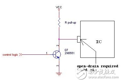
1. The principle of open drain and open set is similar. In many applications we use open collector circuits instead of open drain circuits. For example, an input Pin is required to be driven by an open drain circuit. Then our common driving method is to use a triode to form an open circuit to drive it, which is convenient and cost-effective. As shown in Figure 3.
2. The value of the pull-up resistor R pull-up determines the speed of the edge of the logic level transition. The larger the resistance, the lower the speed and the lower the power consumption. vice versa.
The Push-Pull output is the so-called push-pull output. It should be more suitable than the CMOS output in the CMOS circuit, because the push-pull output capability in CMOS cannot be made as large as the bipolar. Output capacity See the area of ​​the IC's internal output pole N tube P tube. Compared with the open-drain output, the high-low level of push-pull is low by the power supply of the IC, and it is not easy to do logic operations. Push-pull is the most widely used output stage design in CMOS circuits.
Of course, open drain is not without cost, which is the poor drive capability of the output. The statement that the output drive capability is poor is not accurate, and the drive capability depends on the power of the final stage transistor in the IC. OD only brings the delay of the rising edge, because the rising edge charges the load through the external pull-up passive resistor. When the resistance is selected, the time delay is small, but the power consumption is large, and the delay is large. OPEN DRAIN provides a flexible output method, but it also comes at a price. If there is a requirement for delay, it is recommended to use a falling edge output.
The premise that the small delay of the resistor is small is that the principle of resistor selection should be within the allowable range of the power consumption of the final transistor. An experienced designer does not select a 1 ohm resistor as the pull-up resistor when using the logic chip. On the rising edge of the pulse, the power supply charges the load through the pull-up passive resistor. Obviously, the smaller the resistance, the shorter the rise time. On the falling edge of the pulse, in addition to the discharge of the load through the active transistor, the power supply also passes through the pull-up resistor and is turned on. The problem that the transistor forms a path to the ground is the power consumption and power consumption of the chip. The resistance affects the rising edge and does not affect the falling edge. If the rising edge is not used during use, the pull-up resistor can be selected as large as possible to reduce the current to the ground path. If the rising edge time is required, the choice of resistor size should be based on the chip power consumption.
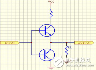
Second, push-pull (Push-Pull) output: 1, what is push-pull?Generally speaking, the two triodes are controlled by two complementary signals, and the other triode is always turned off when one transistor is turned on, which just forms a push-pull connection. Such circuits are also known as push-pull or Totem-pole circuits. The push-pull circuit is suitable for low voltage and high current applications and is widely used in switching power supplies and power amplifier circuits. The simplified circuit diagram is as follows:
The utility model has the advantages that the structure is simple, the magnetic utilization rate of the switching transformer core is high, and when the push-pull circuit works, only two conductive power switches are turned on at a time, so the conduction loss is small.
The disadvantage is: the transformer has a center tap, and the withstand voltage of the switch tube is high; due to the leakage inductance of the primary side of the transformer, the moment the power switch tube is turned off, the drain source will generate a large voltage spike, and the input current The ripple is large and the input filter is bulky.
3, to understand the push-pull output, we must first understand the principle of the transistor (transistor).The triode below has three ports, a base, a collector, and an emitter. The figure below is an NPN transistor.
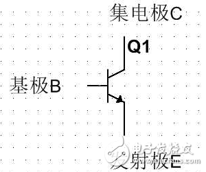
This triode is a current-controlled component, pay attention to keyword current control. This means that this transistor can be controlled as long as the base B has an input (or output) current.
Let me change the concept below, considering base B as the control end, collector C as the input, and emitter E as the output. Here the input and output refers to the direction in which the current flows.
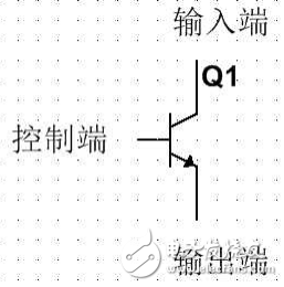
When the control terminal has a current input, a current flows from the input terminal and flows out from the output terminal.
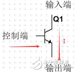
The PNP tube is just the opposite. When a current flows from the control terminal, current flows from the input to the output.
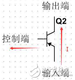
Then push-pull circuit:
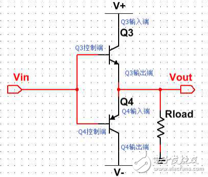
The upper triode is an N-type triode, and the lower triode is a P-type triode. Please pay attention to the control terminal, input terminal and output terminal.
When the Vin voltage is V+, the upper N-type transistor control terminal has a current input, and Q3 is turned on, so that the current passes from top to bottom, and current is supplied to the load.
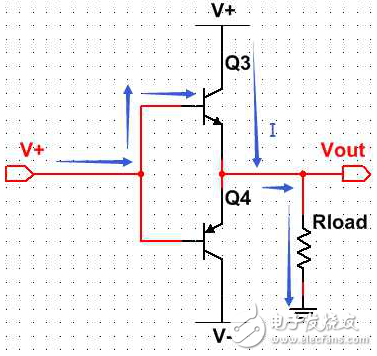
After the above N-type transistor provides current to the load (Rload), this is called "push".
When the Vin voltage is V-, the current triode has current flowing out, Q4 is turned on, and current flows from top to bottom.
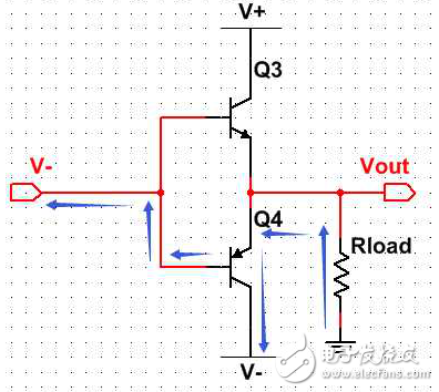
The current P-type transistor provides current to the load (Rload), which is called "pull".
Above, this is the push-pull circuit.
4, push-pull output exampleThe I/O interface of the traditional 8051 MCU can only be used as a standard bidirectional input/output interface. If it is used to drive the LED, it can only be used to sink current or use a triode to expand the drive circuit. The current sinking method is to connect the positive pole of the LED to the VCC, and the negative pole is connected to the I/O interface. When the I/O interface is at a high level, the levels of the two poles of the LED are the same, there is no current, and the LED is turned off. When the I/O interface is low, current flows from VCC to the I/O interface and the LED illuminates. When the positive pole of the LED is connected to the I/O interface, the negative pole is connected to GND, and the I/O interface is set to the high level, the LED will be lit, but the brightness is not ideal due to insufficient pull-up capability of the I/O interface. Push-pull mode of operation is a way of working with strong pull-up capability, which can drive LEDs at a high level. Surprise appeared, connect the positive and negative LEDs to the two I/O interfaces, then set the positive I/O interface to push-pull output, and the negative I/O interface to standard bidirectional sink current input. What happens? What? Very good, we can drive the LED directly with the I/O interface without VCC and GND. LED dot matrix screen is the array connection of multiple LEDs, as long as all the pins of the LED dot matrix screen are connected to the I/O interface, and then according to the pin definition of the LED dot matrix screen, the I/O interface corresponding to the positive pole is set. Push-pull, set the I/O interface corresponding to the negative pole to the standard bidirectional input, and the rest is to give the high and low levels of the row and line corresponding to the points on the LED dot matrix screen to be lit, then everything is under control. Among them.
KNM5 Series Moulded Case Circuit Breaker
KNM5 series Moulded Case Circuit Breaker is MCCB , How to select good Molded Case Circuit Breaker suppliers? Korlen electric is your first choice. All moulded Case Circuit Breakers pass the CE.CB.SEMKO.SIRIM etc. Certificates.
Moulded Case Circuit Breaker /MCCB can be used to distribute electric power and protect power equipment against overload and short-current, and can change the circuit and start motor infrequently. The application of Moulded Case Circuit Breaker /MCCB is industrial.
Korlen electric also provide Miniature Circuit Breaker /MCB. Residual Current Circuit Breaker /RCCB. RCBO. Led light and so on .
KNM5 series Molded Case Circuit Breaker,Small Size Molded Case Circuit Breaker,Electrical Molded Case Circuit Breaker,Automatic Molded Case Circuit Breaker
Wenzhou Korlen Electric Appliances Co., Ltd. , https://www.zjmoldedcasecircuitbreaker.com
