The design of light intensity monitoring system based on TSL256x series sensors
TSL2560 and TSL2561 are high-speed, low-power, wide-range, programmable and flexible configuration light intensity digital conversion chips launched by TAOS. The chip can be widely used in the monitoring of various display screens. The purpose is to make the display screen provide the best display brightness and reduce power consumption as much as possible under changing lighting conditions; it can also be used for street lighting control and safety lighting. And many other occasions. The main features of the chip are as follows:
â—‡ Programmable setting of the upper and lower thresholds of permitted light intensity, and an interrupt signal is given when the actual illuminance exceeds the threshold;
â—‡ The digital output conforms to the standard SMBus (TSL2560) and I2C (TSL2561) bus protocol;
â—‡ Programmable control of analog gain and digital output time;
◇ 1.25 mm×1.75 mm ultra-small package, in low power consumption mode, the power consumption is only 0.75 mW;
â—‡ Automatically suppress 50 Hz/60 Hz light fluctuations.
2 Pin function of TSL256xTSL256x has 2 types of packages: 6LEAD CHIPSCALE and 6LEAD TMB. The encapsulation form is different, the corresponding illuminance calculation formula is also different. Figure 1 shows the pin layout of these two packages.

Figure 1 TSL256x package
The functions of each pin are as follows:
Pin 1 and Pin 3: Power pin and signal ground respectively. Its working voltage range is 2.7~3.5V.
Pin 2: Device access address selection pin. Due to the different levels of this pin, the device has 3 different access addresses. The corresponding relationship between the access address and the level is listed in Table 1.
Table 1 Correspondence between device access address and pin 2 level

Pin 4 and Pin 6: I2C or SMBus bus clock signal line and data line.
Pin 5: Interrupt signal output pin. When the light intensity exceeds the upper or lower threshold set by the user, the device will output an interrupt signal.
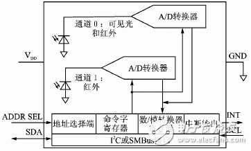
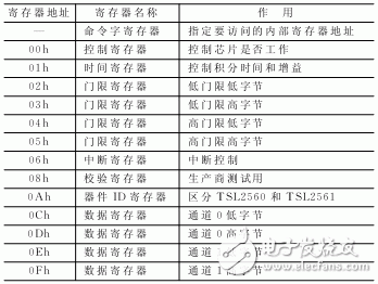
3 Internal structure and working principle of TSL256xTSL256x is the second-generation ambient light intensity sensor, and its internal structure is shown in Figure 2. Channel 0 and channel 1 are two photodiodes, in which channel 0 is sensitive to both visible light and infrared, while channel 1 is only sensitive to infrared. The integral A/D converter integrates the current flowing through the photodiode and converts it into a digital quantity. After the conversion is completed, the conversion result is stored in the respective registers of channel 0 and channel 1 inside the chip. When an integration period is completed, the integral A/D converter will automatically start the next integral conversion process. The microcontroller and TSL2560 can be implemented through standard SMBus (System Management Bus) V1.1 or V2.0, and TSL2561 can be accessed through the I2C bus protocol. The control of TSL256x is realized by reading and writing to its internal 16 registers, its address is listed in Table 2.

Figure 2 TSL256x internal structure diagram
Table 2 TSL256x internal register address and function

The access of TSL256x follows the standard SMBus and I2C protocol, which makes the chip hardware and software design very simple. Although the read and write timings of these two protocols are very similar, there are still differences. The following only takes the TSL2561 chip as an example to illustrate the practical application of the TSL256x light intensity sensor.
4.1 Hardware design
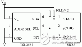
TSL2561 can be accessed through the I2C bus, so the hardware interface circuit is very simple. If the selected microcontroller has an I2C bus controller, connect the clock line and data line of the bus directly to the SCL and SDA of the I2C bus of TSL2561 respectively; if there is no pull-up resistor inside the microcontroller, you also need Use two pull-up resistors to connect to the bus. If the microcontroller does not have an I2C bus controller, just connect the SCL and SDA of the I2C bus of TSL2561 to the ordinary I/O port; however, when programming, you need to simulate the timing of the I2C bus to access TSL2561, and the INT pin is connected to the micro controller. External interrupt of the device. The hardware connection is shown in Figure 3.

Figure 3 The hardware connection diagram of the microcontroller and TSL2561
4.2 Software design
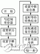
The microcontroller can read and write TSL2561 through the I2C bus protocol. When writing data, send the device address first, and then send the data to be written. The write operation process of TSL2561 is as follows: First send a group of device addresses; then write the command code. The command code specifies the address 00h~0fh of the register and the way of writing the register. It is byte, word or block (several words). ) Is the unit for writing; the data to be written is finally sent. According to the way of writing the register specified by the previous command code, the data to be written can be sent continuously, and the internal write register will automatically increase by 1. For the specific read and write timing of the I2C protocol, you can refer to related materials, so I won't repeat them here. The software design flow of TSL2561 is shown as in Fig. 4.

Figure 4 Software design process
Due to space limitations, here are some procedures for reading and writing to TSL2561:
unsigned char TSL2561_write_byte (unsigned char addr, unsigned char c) {
unsigned char status=0;
status=twi_start();//start
status=twi_writebyte(TSL2561_ADDR|TSL2561_WR);//write TSL2561 address
status=twi_writebyte(0x80|addr);//write command
status=twi_writebyte(c);//write data
twi_stop( );//stop
delay_ms(10);//delay 10 ms
return 0;
}
unsigned char TSL2561_read_byte (unsigned char addr, unsigned char *c) {
unsigned char status=0;
status = twi_start( );//start
status=twi_writebyte(TSL2561_ADDR|TSL2561_WR);//write TSL2561 address
status=twi_writebyte(0x80|addr);//write command
status=twi_start( );//Restart
status=twi_writebyte(TSL2561_ADDR|TSL2561_RD);//write TSL2561 address
status=twi_readbyte(c, TW_NACK);//write data
twi_stop( );
delay_ms(10);
return 0;
}
When the integral A/D converter is converted, the corresponding values ​​CH0 and CH1 can be read from the channel 0 register and channel 1 register, but the unit should be Lux (lumens), and the calculation should be based on CH0 and CH1. For the TMB package, assuming that the light intensity is E (in Lux), the calculation formula is as follows:
①0《CH1/CH0≤0.50
E=0.030 4×CH0-0.062×CH0×(CH1/CH0)1/4
② 0.50《CH1/CH0≤0.61
E=0.022 4×CH0-0.031×CH1
③ 0.61《CH1/CH0≤0.80
E=0.012 8×CH0-0.015 3×CH1
④ 0.80《CH1/CH0≤1.30
E=0.001 46×CH0-0.001 12×CH1
⑤ CH1/CH0》1.30
E=0
For the CHIPSCALE package, the calculation formula can be found in the corresponding chip information.
5 ConclusionThe system that uses TSL256x to realize real-time monitoring of light intensity has the advantages of high accuracy, low cost, and small size. The chip integrates an integral A/D converter and uses digital signal output, so the anti-interference ability is stronger than similar chips. This chip has been widely used in the field of light intensity monitoring and control.
Automotive Diagnostic Connectors And Cables
We make OBD connector with terminal by ourselves, soldering type and crimping type are both available. Such as 16pin obd connector. OBD1, OB2, J1939, J1708, J1962, etc. Also molded by different type, straight type or right-angle type. The OBD connector cables used for Audi, Honda, Toyota, BWM, etc. We have wide range of materials source , also we can support customers to make a customized one to replace the original ones.
Automotive Diagnostic Connectors And Cables,Obd Connectors,Reliable OBD Connector,Black OBD Connector,OBD Diagnostic Cable,OBD2 Connectors
ETOP WIREHARNESS LIMITED , https://www.etopwireharness.com
