BGA packaging technology for embedded design is steadily advancing
[Lizhi Technology: High-speed RF PCB design well-known brand]
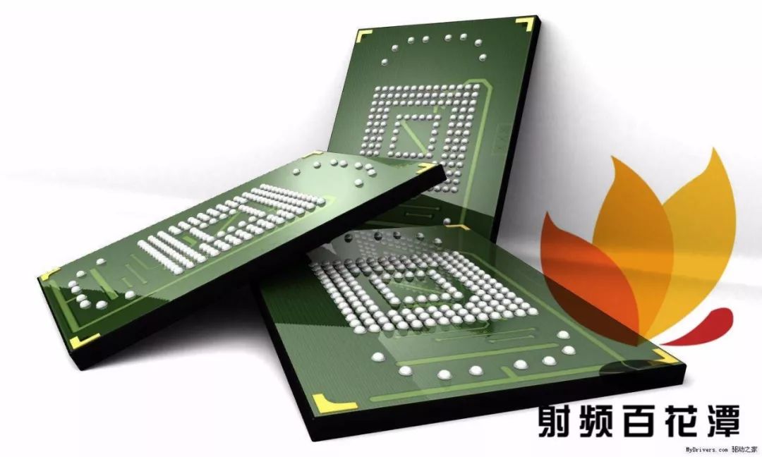
The first task of the embedded designer is to develop a suitable fan-out strategy to facilitate the manufacture of the circuit board. The key factors that need to be considered when choosing the correct fan-out/wiring strategy are: ball pitch, contact diameter, number of I/O pins, via type, land size, trace width and spacing, and detour from BGA The number of layers required.
And embedded designers always require the use of the least number of circuit board layers. In order to reduce costs, the number of layers needs to be optimized. But sometimes designers must rely on a certain number of layers. For example, in order to suppress noise, the actual wiring layer must be sandwiched between two ground plane layers.
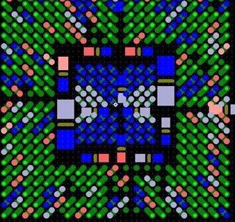
Figure 1: Dog bone fanout
In addition to these design factors inherent in the embedded design based on a specific BGA, the main part of the design also includes two basic methods that the embedded designer must take to correctly route the signal from the BGA: Dog bone fan-out (Figure 1) And vias in the pad (Figure 2). Dog bone fan-out is used for BGAs with ball pitches of 0.5mm and above, while vias in pads are used for BGAs and micro-BGAs with ball pitches below 0.5mm (also called ultra-fine pitch). Pitch is defined as the distance between the center of a certain ball of the BGA and the center of adjacent balls.
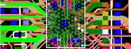
Figure 2: Fan-out method of vias in pads
It is important to understand some basic terms related to these BGA signal routing technologies. The term "via" is the most important. Vias refer to pads with plated holes. This plated hole is used to connect copper wires on a certain PCB layer and copper wires on another layer. High-density multilayer circuit boards may use blind or buried vias, also known as micro vias. Only one side of the blind hole is visible, and both sides of the buried hole are not visible.
Dog bone fanout
The fan-out method of the BGA type is divided into 4 quadrants, and a wider channel is left in the middle of the BGA for laying out multiple traces from the inside. Breaking down the signals from the BGA and connecting them to other circuits involves several key steps.
The first step is to determine the via size required for BGA fan-out. Via size depends on many factors: device spacing, PCB thickness, and the number of traces that need to be routed from one area or perimeter of the via to another area or perimeter. Figure 3 shows three different perimeters related to BGA. The perimeter is a polygonal boundary defined as a matrix or square surrounding the BGA ball.
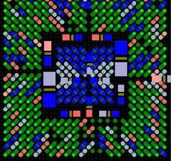
Figure 3: Three different perimeters related to BGA. (Perimeter: Perimeter)
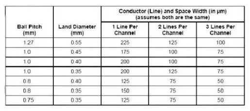
The dashed lines passing through the first row (horizontal) and corresponding to the first column (vertical) form the first perimeter, followed by the second and third perimeters. The designer starts wiring from the outermost perimeter of the BGA, and then keeps going inward until the innermost perimeter of the BGA ball. The size of the via is calculated from the contact diameter and the ball pitch, as shown in Table 1. The contact diameter is also the pad diameter of each BGA ball.
Table 1: Use contact diameter and ball spacing to calculate via size. (Note: Ball pitch: Ball pitch)
Land Diameter: Contact diameter
conductor (Line) and space width (in μm): conductor (line) and space width (within μm)
Assumes both are the same: Assumes both are the same
1 Line per channel: 1 line per channel
2 lines per channel: 2 lines per channel
Once the Dog bone fan-out is completed and the specific via pad size is determined, the second step is to define the trace width from the BGA to the inner layer of the circuit board. There are many factors to consider when confirming the trace width. Table 1 shows the trace width. The minimum space required between traces limits the BGA detour routing space. It is important to know that reducing the space between traces will increase circuit board manufacturing costs.
The area between the two vias is called the routing channel. The channel area between adjacent via pads is the minimum area through which signal routing must pass. Table 1 is used to calculate the number of traces that can be routed through this area.
As shown in Table 1, when implementing BGA signal detour routing, the trace width and minimum space requirements between traces must be met. The channel area between adjacent via pads is the minimum area through which signal routing must pass.
Channel area CA=BGA pitch-d, where d is the diameter of the via pad.
Table 2 calculates the number of traces that can be routed through this area.
Table 2: Calculate the number of traces passing through a given channel area. (Note: Number of Traces: Number of Traces)

Formula: formula;
Space width: space width;
Trace width: trace width.
Many traces can be routed through different channels. For example, if the BGA pitch is not very fine, one or two traces can be deployed, sometimes three. For example, for a 1mm pitch BGA, multiple traces can be deployed. However, with today's advanced PCB design, most of the time there is only one trace for a channel.
Once the embedded designer determines the trace width and spacing, the number of traces routed through a channel, and the type of vias used for BGA layout design, he or she can estimate the number of PCB layers required. Using less than the maximum number of I/O pins can reduce the number of layers. If wiring is allowed on the first and second layers, then the wiring on the two outer perimeters does not need to use vias. The other two perimeters can be routed on the bottom layer.
In the third step, the designer needs to maintain impedance matching as required and determine the number of wiring layers to be used to completely decompose the BGA signal. Next, use the top layer of the circuit board or the layer where the BGA is placed to complete the wiring of the BGA outer ring.
The remaining internal parameters are distributed on the internal wiring layer. According to the number of internal wiring in each channel, it is necessary to fairly estimate the number of layers required to complete the entire BGA wiring.
After the wiring of the outer ring is completed, lay out another round. The set of diagrams in Figure 4a and Figure 4b describe how PCB designers route different BGA circles, starting from the outermost and all the way to the center. The first picture shows how the first and second inner rings are wired. Then follow the same method to wire the subsequent inner ring until all BGA wiring is completed.
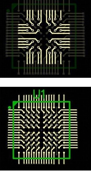
Figure 4a and 4b: How to route the different BGA circles, starting from the outermost layer and reaching the center
In some designs that need to consider electromagnetic interference (EMI), the outer layer or top layer cannot be used for wiring, even the outer ring. In this case, the top layer serves as a ground plane. EMI includes the susceptibility of a product to external electromagnetic fields, and external electromagnetic fields generally enter another product from one product through coupling or radiation, and often cause the latter product to fail the conformance test. Products must meet the following three standards to be considered to meet the requirements of electromagnetic compatibility specifications:
Does not interfere with other systems;
Not affected by radiation from other systems;
Will not interfere with itself.
In order to prevent the product from sending and receiving interference signals, it is recommended to take shielding measures for the product. Shielding generally refers to completely enclosing the entire electronic product or part of the product with a metal shell. However, in most cases, filling the outer layer with a ground plane can also act as a shield because it can attract energy and minimize interference.
In-pad via technology for ultra-fine pitch
When using the in-pad via technology for BGA signal escape and routing, the via is directly placed on the BGA pad and filled with conductive material (usually silver) to provide a flat surface.
The example of fan-out via holes in the micro-BGA pad used in this article uses 0.4mm ball or lead pitch. The PCB is 18 layers, including 8 signal wiring layers. BGA wiring usually requires more layers. But in this example, the number of layers is not a problem, because only a few BGA balls are used. The key issue is still the 0.4mm narrow pitch of the micro BGA, and the top layer does not allow wiring except for fan-out. The goal is to fan out the micro-BGA without negatively affecting PCB manufacturing.
Figure 5 shows the outline drawing provided by the BGA device manufacturer. As you can see from the figure, the recommended pad size is 0.3mm (12mil), and the lead pitch is 0.4mm (16mil). Due to the extremely small spacing between the pads, it is impossible to realize the traditional Dog bone fan-out pattern. Even small vias cannot be used for Dog bone fan-out strategies. The small size vias here mean 6mil drill holes and 10mil ring pads. Another important mechanical limitation is the board thickness, which in this case is 93 mils.
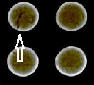
Figure 5: Outline drawing provided by BGA device manufacturer
In this case, the most convenient solution is to use micro vias in the pad. However, the size of the micro vias cannot exceed 3 mils. But the board thickness of 93mil is a limiting factor. Another option is blind via and buried via technology. But these options will limit the choice of manufacturing technology and increase costs.
In order to be able to choose different manufacturing companies, the hole size in the 93mil-thick circuit board cannot be less than 6mil, and the trace width cannot be less than 4mil. Otherwise, only a few high-end circuit board manufacturers can take over this project, and it is expensive. Figure 6 shows the BGA outline drawing related to this example.
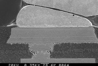
Figure 6: This fan-out method avoids the use of high-end technology and does not affect signal integrity. BGA pins are divided into internal pins and external pins
The fan-out method shown in Figure 6 avoids the use of high-end technology and does not affect signal integrity. BGA pins are divided into two parts, internal and external pins. In-pad vias are used internally, and external pins are fanned out on a 0.5mm grid. Figure 7a shows the top layer, and Figure 7b shows the top layer and internal wiring layers.
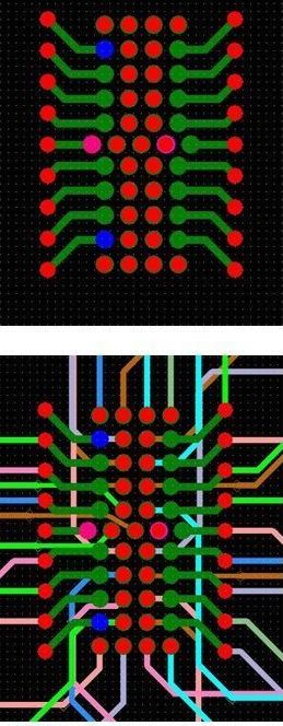
Figures 7a and 7b: In-pad vias are used for the inside, while external pins are fanned out on a 0.5mm grid. Figure 7a shows the top layer; Figure 7b shows the top layer and internal wiring layers.
Since the BGA pad size is 0.3mm (12mil) and the pitch is 0.4mm (16mil), a 6/10mil via (hole/ring size) is used in the pad. The external expansion fan-out uses the same via. Inside, the gap between vias is 6mil, which is a standard size and will not cause manufacturing problems. The external via gap is 10mil. This gap can take a 3mil line, and the distance between the line and the via is 3.34mil. This special strategy allows all signals from the 0.4mm pitch micro BGA to be successfully fan-out without any special manufacturing requirements.
Regardless of whether you are using Dog bone or the method of in-pad vias, the basic steps are the same, that is, you must first determine the correct channel space, including defining the size of vias and pads, trace width, impedance requirements, and stackup. However, the difference lies in the via arrangement and the via group used.
It is recommended to use blind/buried vias with a depth of up to 6 layers. More layers will cause manufacturing yield problems. The preferred technique is to use crossed vias or stacked vias, as shown in Figure 8. Crossed vias allow for more precise registration tolerances because they do not enforce perfect alignment like stacked vias.
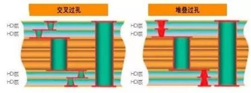
Figure 8: Crossed vias allow larger registration tolerances because they do not enforce perfect alignment like stacked vias
What would go wrong without these steps
Whether using Dog bone or via-in-pad technology, manufacturability and functionality are two important aspects that need to be carefully considered. The key is to know the manufacturing limits of the manufacturing plant. Some factories can produce particularly strict designs. However, if the product is ready for mass production, the cost will be high. Therefore, it is particularly important to consider the selection of ordinary manufacturing plants when designing.
In short, the key factors to be considered from a manufacturing perspective are:
Cascade
Via-hole size (depending on the aspect ratio)
Via-hole ring (minimum 3mi required)
Vias-stacked (stacked or crossed)
Copper foil to copper foil distance (recommended minimum 3mil)
Copper foil to drilling distance (minimum 5mil required)
BGA contact size and solder ball size for assembly
There is always a compromise between manufacturability and functionality. Therefore, it is critical to analyze each aspect correctly and then make the appropriate decision.
On the other hand, functions include signal integrity, power distribution and electromagnetic compatibility. These can be divided into the following categories:
The key to reflection and transmission lines (a line) is impedance control. Impedance is controlled by trace width, dielectric thickness and reference plane.
The key to reflection and transmission lines (a line) is impedance control. Impedance is controlled by trace width, dielectric thickness and reference plane.
Crosstalk (two or more lines) The distance between traces on the same and adjacent layers is the key to controlling crosstalk. Placing a ground plane between each signal layer and grounding the shielding wire around noise-sensitive or noise-radiating traces helps minimize crosstalk.
Power distribution (rail destruction) This is the inductance of the power network. Adjacent power and ground planes and using decoupling capacitors help control power surges.
Electromagnetic interference (system destruction) controls all the above units, while shielding the entire PCB or the noise-sensitive and noise-producing parts can help control electromagnetic interference.
The above measures are also correct for the entire product. However, it is especially correct in the BGA area, because all the signals and power are very close to each other, which is extremely challenging. A correct understanding of signal characteristics helps to make a decision about which network has higher priority in terms of functionality.
Using a large ground plane in the layer close to the BGA helps to solve most signal integrity problems. One of the biggest benefits of blind vias is that the branch length is eliminated in blind/buried vias, which is especially important for high-frequency signals.
Summary of this article
BGA packaging technology for embedded design is advancing steadily, but it is still very difficult and extremely challenging to route signals around. There are several key factors to consider when choosing the correct fan-out/wiring strategy: ball pitch, contact diameter, number of I/O pins, via type, pad size, trace width and spacing, and stackup. Following some of the strategies described in this article can ensure that the product has the correct form, assembly and function.
Wireless Bridge,Wifi Wireless Bridge,Gigabit Wifi Bridge,Long Range Wifi Bridge
Shenzhen MovingComm Technology Co., Ltd. , https://www.movingcommiot.com
