Detailed explanation of jtag working principle
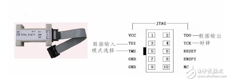
JTAG (Joint Test AcTIon Group) is an international standard test protocol (IEEE 1149.1 compliant). The standard JTAG interface is 4-wire - TMS, TCK, TDI, TDO, which are mode selection, clock, data input and data output lines.
JTAG is one of the most basic communication protocols. You can understand that it is the same as RX TX or USB. It is just a communication method, but it is very different from RX TX and USB. That is, this JTAG protocol is the most The bottom layer, said a little more popular, in general, inside the phone, the CPU is the boss, right? But in front of JTAG, he is not the boss, the JTAG protocol is used to control the CPU, in the face of JTAG CPU becomes paralyzed. The general protocol is to ask the CPU to read and write the font library, but JTAG can read and write the CPU program, the command allows the CPU to work all the time, the thief first smashes the king, JTAG is the dragon knife.

JTAG is also an international standard test protocol (IEEE 1149.1 compliant), mainly used for on-chip testing. Most advanced devices now support JTAG protocols such as DSPs and FPGA devices. The standard JTAG interface is 4-wire: TMS, TCK, TDI, TDO, which are mode selection, clock, data input, and data output lines. The related JTAG pins are defined as: TCK is the test clock input; TDI is the test data input, the data is input to the JTAG interface through the TDI pin; TDO is the test data output, and the data is output from the JTAG interface through the TDO pin; TMS is the test mode selection TMS is used to set the JTAG interface to a specific test mode; TRST is a test reset, input pin, active low
There are two main functions of JTAG, or JTAG mainly has two major categories: one for testing the electrical characteristics of the chip, detecting whether the chip has a problem; the other is for debugging, debugging various types of chips and their peripheral devices. . A CPU with a JTAG Debug interface module can access the internal registers of the CPU, the devices attached to the CPU bus, and the registers of the built-in modules through the JTAG interface as long as the clock is normal. This article mainly introduces the Debug function.
Note: JTAG can access some internal registers, mainly registers in the CPU, such as some general-purpose registers, etc.; also can access some devices hanging on the bus, such as on-chip memory L1, L2, L3, etc.; also can access the built-in module Registers, such as the MMU module, can be accessed through JTAG.
1 JTAG principle analysisSimply put, the working principle of JTAG can be summarized as: a TAP (Test Access Port) is defined inside the device, and internal nodes are tested and debugged through a dedicated JTAG test tool. First introduce the basic concepts and content of boundary scan and TAP.
1.1 Boundary ScanThe basic idea of ​​Boundary-Scan technology is to add a shift register unit, the Boundary-Scan Register, to the input/output pins close to the chip.
When the chip is in the debug state, the boundary scan register isolates the chip from the peripheral input/output. Observation and control of the chip input/output signals can be achieved by the boundary scan register unit. For the input pin of the chip, the signal (data) can be loaded into the pin through the boundary scan register unit connected thereto; for the output pin of the chip, it can also be "captured" by the boundary scan register connected thereto. The output signal on this pin. In the normal operating state, the boundary scan register is transparent to the chip, so normal operation will not be affected. In this way, the Boundary Scan Register provides a convenient way to observe and control the chips that need to be debugged. In addition, the boundary scan (shift) register units on the chip input/output pins can be connected to each other to form a boundary scan chain (Boundary-Scan Chain) around the chip. The boundary scan chain can be serially input and output, and the chip in the debug state can be conveniently observed and controlled by the corresponding clock signal and control signal.
1.2 Test Access TAPThe TAP (Test Access Port) is a general-purpose port that provides access to all data registers (DRs) and instruction registers (IRs) provided by the chip. Control of the entire TAP is done through the TAP Controller. Let's first introduce the several interface signals of TAP and their functions. Among them, the first four signals are mandatory in the IEEE1149.1 standard.
â—‡TCK: The clock signal provides an independent, basic clock signal for the operation of the TAP.
â—‡TMS: Mode select signal for controlling the conversion of the TAP state machine.
â—‡TDI: Data input signal.
â—‡TDO: Data output signal.
â—‡TRST: Reset signal, which can be used to reset (initialize) the TAP Controller. This signal interface is not mandatory in the IEEE 1149.1 standard because the TAP Controller can also be reset via TMS.
â—‡STCK: Clock return signal, not mandatory in the IEEE 1149.1 standard.
â—‡ DBGRQ: Control signal for the working state on the target board. There is no requirement in the IEEE 1149.1 standard, but only in individual target boards (eg STR710).
Simply put, the PC debugs the target board by accessing the relevant data registers (DR) and instruction registers (IR) through the TAP interface.
After the system is powered on, the TAP Controller first enters the Test-LogicReset state, and then enters Run-Test/Idle, Select-DR-Scan, Select-IR-Scan, Capture-IR, Shift-IR, Exitl-IR, Update-IR. State, and finally return to the Run-Test/Idle state. In this process, the state transition is driven by the TCK signal (rising edge), and the state of the TAP is selectively converted by the TMS signal. Among them, in the Capture-IR state, a specific logic sequence is loaded into the instruction register; in the Shift-IR state, a specific instruction can be sent to the instruction register; in the Update-IR state, just input to The instructions in the instruction register will be used to update the instruction register. Finally, the system returns to the Run-Test/Idle state, the instruction takes effect, and access to the instruction register is completed. When the system returns to the Run-Test/Idle state, the required data register is selected according to the contents of the previous instruction register, and the operation of the data register is started. The basic principle is exactly the same as the access of the instruction memory, followed by Select-DR-Scan, Capture-DR, Shift-D, Exit1-DR, Update-DR, and finally back to the Run-Test/Idle state. With TDI and TDO, new data can be loaded into the data registers. After one cycle, the data in the data register can be captured, the data update of the chip pins connected to each register unit of the data register is completed, and the access to the data register is completed.
Currently, the JTAG interface on the market is available in 14-pin and 20-pin versions. Among them, the 20-pin is the mainstream standard, but there are also a few target boards that use 14-pin. After a simple signal conversion, they can be used universally.
Laptop Standing Desk Adjustable,Laptop Standing Desk Adjustable Height,Laptop Standing Desk Cart,Laptop Standing Desk Foldable,etc.
Shenzhen Chengrong Technology Co.ltd is a high-quality enterprise specializing in metal stamping and CNC production for 12 years. The company mainly aims at the R&D, production and sales of Notebook Laptop Stands and Mobile Phone Stands. From the mold design and processing to machining and product surface oxidation, spraying treatment etc ,integration can fully meet the various processing needs of customers. Have a complete and scientific quality management system, strength and product quality are recognized and trusted by the industry, to meet changing economic and social needs .

Laptop Standing Desk Adjustable,Laptop Standing Desk Adjustable Height,Laptop Standing Desk Cart,Laptop Standing Desk Foldable
Shenzhen ChengRong Technology Co.,Ltd. , https://www.dglaptopstandsupplier.com
