FPGA implementation design of AIS non-coherent demodulation software receiver based on band-pass sampling
The AIS system is a ship traffic information exchange system. The shipborne AIS equipment continuously sends its own information, such as heading, tonnage, etc., to guide the dispatch and avoid collisions. With the rapid growth of maritime trade, there is an urgent need to establish a real-time monitoring system for ship dynamics in large areas of sea, and satellite platforms are valued because of their wide coverage. Countries such as Canada have successively launched satellites carrying AIS signal receiving equipment. The AIS system adopts Gaussian Filtered Minimum Shift Keying (GMSK) modulation, which can be demodulated in a coherent or non-coherent manner. Coherent demodulation has good anti-noise performance, but it needs to recover the carrier frequency accurately. The orbital height of the near-Earth satellite carrying AIS equipment is generally about 500 km, and the Doppler frequency shift can reach ±4 kHz, so the accurate carrier Recovery is more difficult; incoherent demodulation mainly uses frequency discriminators to extract frequency change information from the received GMSK signal, so it is insensitive to frequency offset and has a simple structure. It has been applied in many GMSK mobile communication systems, such as GSM. At present, the RF end of the AIS receiver mostly adopts a one-level or two-level down-conversion scheme, which makes the radio frequency front-end hardware more complicated and the hardware cost is high. In view of the fact that the AIS signal is a narrowband signal, the received radio frequency signal is directly bandpass sampled in the design of this article to simplify the receiver hardware structure.
The main work of this paper is as follows: A band-pass sampling-based AIS non-coherent demodulation software receiver is designed on Xilinx xc4vlx80 FPGA, and the design file is downloaded to the FPGA after comprehensive mapping. The actual AIS signal source is used as the test signal through embedded logic. The analysis tool Chipscope observes the internal signals of the FPGA on the PC to verify the design and gives the hardware resource consumption.
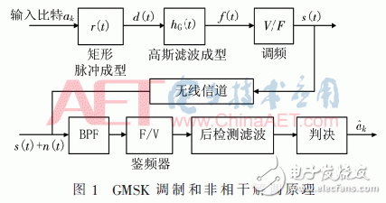
1 Principle of GMSK signal modulation and non-coherent demodulationThe AIS signal is a GMSK modulated signal, and the modulation and non-coherent demodulation process is shown in Figure 1.
The bit pulse at the transmitting end is:

The bit stream d(t) is pulse-shaped by a Gaussian filter with BbTb (Bandwidth-TIme product, BT). Bb is the 3 dB bandwidth of the Gaussian filter, and Tb is the bit rate. The impulse response of the Gaussian shaping filter is:

Where * means convolution operation. Finally, through voltage/frequency (V/F) conversion, a frequency modulation signal is formed and modulated to a specified frequency band for transmission.
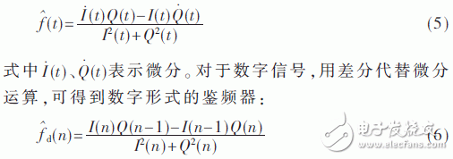
For the receiver of non-coherent demodulation, the received signal is first subjected to quadrature down-conversion, high frequency components and out-of-band noise are filtered out to obtain baseband quadrature signals I(t), Q(t), and then the frequency is calculated by the following formula /Voltage (F/V) conversion:
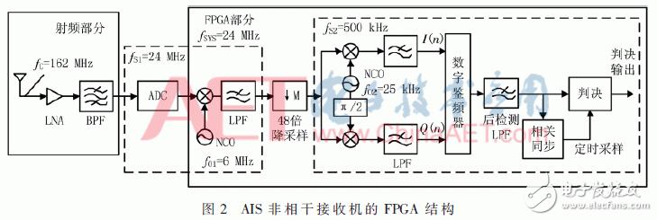
The system structure of the band-pass sampling AIS incoherent receiver is shown in Figure 2.
2.1 Bandpass sampling rate
The AIS signal has two radio frequency points A and B, which are 161.975 MHz and 162.025 MHz, respectively. The data rate Rb is 9.6 kb/s, and the bandwidth does not exceed 25 kHz. The band pass filter (Band Pass Filter, BPF ) The center frequency is 162 MHz and the bandwidth is 250 kHz, so the BPF output RF signal can be directly sampled. Theoretically, the ADC band-pass sampling frequency fS1 only needs to satisfy the following formula:

In the formula, B is the bandwidth of BPF, fH is the highest frequency component of the sampled signal, [] represents the largest integer that does not exceed this number. The smaller the sampling frequency, the lower the processing speed requirement of FPGA. However, in the actual system, due to the slow-changing characteristics of the BPF transition band, some sideband noise cannot be completely suppressed. When the sampling frequency is too small, the frequency spectrum of the sampled signal overlaps too many times, which causes more noise to be superimposed on the useful signal. Therefore, the sampling clock frequency adopted by this system is fS1=24 MHz. After bandpass sampling, the center frequency fC1 of the AIS signal can be calculated by the following formula:

2.2 Two-stage digital down-conversion structure
FPGA and ADC share the clock source in the system, and the main frequency of FPGA system is fSYS=24 MHz. The AIS signal received by the antenna is low-noise amplifier and band-pass filtered, and then sampled by a 14-bit ADC before being input to the FPGA. The center frequency of the AIS signal input to the FPGA is fC1=6 MHz, the sampling rate fS1=24 MHz, and the bandwidth is 250 kHz. Since the signal bandwidth is much smaller than the sampling frequency, down-conversion and down-sampling processing can be performed to reduce the pressure of post-processing. First, the sampled signal is mixed with a sine signal with a bit width of 10 bit and a frequency fO1=6 MHz generated by the numerically controlled oscillation (NCO) IP core in the FPGA, and then through a 51 with a data bit width of 16 bit and a cutoff frequency of 100 kHz. High-order low-pass filter to filter out high-frequency components; then the low-pass signal is down-sampled by 48 times to obtain an AIS signal with a data rate of 500 kHz and a center frequency of ±25 kHz (A and B two radio frequency points) ; Then the signal is mixed with a sine signal with a bit width of 10 bit and a frequency fO2=25 kHz generated by the NCO, and then filtered by a 51-order low-pass filter with a data bit width of 16 bit and a cutoff frequency of 25 kHz In addition to high-frequency components, a baseband quadrature signal containing Doppler frequency deviation (less than 4 kHz) is obtained.
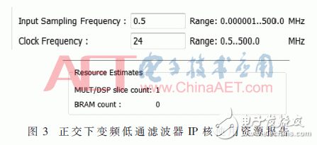
The advantages of using this two-stage down-conversion can not only reduce the sampling rate and reduce the processing pressure of the FPGA, but also reduce the consumption of logic resources. If the signal with sampling rate fS1=24 MHz is directly subjected to quadrature digital down-conversion, because the mixed FIR low-pass filter drives the clock frequency (that is, the system main frequency fSYS=24 MHz) and the mixed signal of the input filter The data rate (ie, the sampling rate is fS1=24 MHz) is the same, so after the FIR filter IP core is synthesized, 26 multipliers are needed. Quadrature down-conversion requires two low-pass filters, so a total of 26&TImes;2=52 multipliers are needed; when a two-stage down-conversion scheme is adopted, the filter after one-stage mixing also needs 26 multipliers, downsampling After that, the data rate of the mixed signal of the input filter is reduced to fS2=500 kHz, and the drive clock remains unchanged at fSYS=24 MHz. Therefore, the multiplier fSYS/fS2 can be multiplexed at most during the input period of one data. =48 times, which is greater than the 26 multipliers required by the 51-order FIR filter, so the filter after the quadrature down-conversion is synthesized, and only one multiplier is needed, as shown in Figure 3. Three low-pass filters are required in the two-stage down-conversion (as shown in Figure 2), but the number of multipliers required is only 26+1&TImes;2=28.
2.3 Digital frequency discrimination and post-detection filtering
Perform the digital frequency discrimination operation shown in equation (6) on the baseband quadrature signal obtained by quadrature down-conversion to extract the frequency signal. The hardware of the digital frequency discriminator is mainly composed of delay module, multiplier, divider, adder and subtractor. Since digital frequency discrimination is a non-linear operation in theory, it is very sensitive to noise, and the output will contain high-frequency noise components, so it is necessary to perform post-detection low-pass filtering on the output of the discriminator. Fig. 4 is the bit error rate curve of AIS demodulation when using low-pass filters with different cut-off frequencies in MATLAB simulation. The abscissa is the ratio of signal power to noise power. It can be seen from the figure that when the cutoff frequency Bo of the low-pass filter is 0.4Rb (Rb is the AIS bit rate), the error performance is the best. Therefore, the bandwidth of post-detection filtering in FPGA is set to 0.4Rb=0.4&TImes;9.6 kb/s=3.84 kHz.

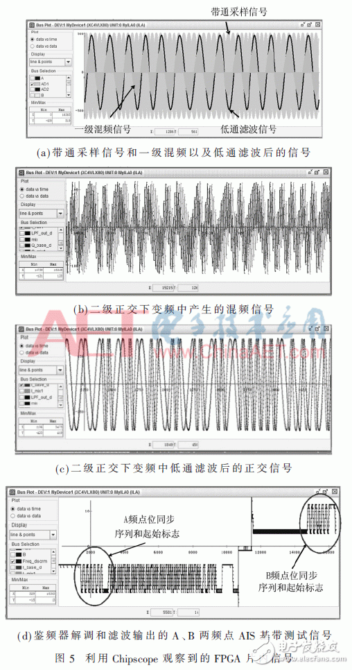
Design each module of the AIS receiver in Xilinx development environment ISE13.2, synthesize, map, place and route the designed modules, and generate download files. And call Chipscope embedded logic analyzer IP core, connect FPGA and PC through JTAG simulator, in order to observe FPGA internal signal in real time. The actual AIS signal source is used as the test signal, and the AIS signal source output is connected to the input of the analog-to-digital converter AD9246 with a coaxial cable, and the band-pass sampling signal is read into the FPGA for demodulation. Observe the signal of all levels as shown in Figure 5. In Figure 5(d), you can see the 24-bit synchronization sequence 00110011...0011 and the frame start flag 01111110 of the AIS signals at two different frequencies of A and B. The number of slices occupied by the design is 231, which only accounts for 1% of the total resources.
Based on the principle of non-coherent demodulation of GMSK signals, this paper designs a band-pass sampling AIS non-coherent receiver on Xilinx FPGA. Using the characteristics of AIS narrowband signals, a two-stage down-conversion scheme is adopted to reduce the data rate to a reasonable range and reduce FPGA handles the pressure, while also greatly reducing the consumption of hardware logic resources by the low-pass filter; the theoretical simulation of AIS demodulation is carried out in MATLAB, and an optimal digital frequency discrimination is set to detect the filter cut-off frequency to suppress Noise interference in the actual environment; Finally, the designed receiver was tested on the hardware system, and the demodulated baseband signals at A and B frequencies were observed. The logic resources consumed by this design are less than 1% of the total device resources, which can provide a reference for the miniaturization and mass production of AIS receivers.
Guiding Cable,Screen Type Guiding Cable,Screen Guiding Cable,Copper Wire Shield Guiding Cable
Baosheng Science&Technology Innovation Co.,Ltd , https://www.bscables.com
