Future battlefield scout robots show great power
The US Army and Marine Corps purchased thousands of different throwing robots for reconnaissance missions inside buildings, caves, and more. The manufacturer of the robot called "Scout" installed a microphone on the robot at the request of the user, which has a strong situational awareness.
The Scout robot is a close-range remote-controlled reconnaissance robot. Compared with the general military robot , its shape is small and alternative. The middle is a titanium alloy axle with a length of 18.6 cm and a diameter of 4 cm. The ends are made of high-strength plastic. The finished wheel with gears weighs only 546 grams. Its shape looks like a dumbbell. The two antennas on the front end are mainly used to receive commands from the remote control. The axle is equipped with batteries and electronics. Its infrared night vision camera has a line of sight of about 8 meters, and the line of sight of the daytime camera is much farther. When the light is dark until the daytime camera is not working properly, the night vision camera will automatically turn on.
As a new reconnaissance robot, its biggest feature is its small size and light weight. It is very suitable for performing long-term monitoring and investigation tasks in a small space, and has strong situational awareness. Users can throw such small robots into darkrooms or caves, and then let them move around, while returning video and sound, which is very helpful for soldiers to perceive the battlefield environment. In Afghanistan, for example, soldiers usually put the robot into a rocky area or throw it to the other side of the wall. After landing, they can be manipulated using the remote control. While the robot is moving fast, the micro camera transmits the captured information to the display of the remote control. In the building, the "scout" image transmission distance is 30 meters; in the outdoor, its transmission distance is three times that of the indoor. The remote control weighs less than 900 grams and comes with a 3.5-inch display with a resolution of 640 x 480.
Gold Fingers PCB -Here's all the information about Goldfinger PCB
Gold Fingers PCB, Gold Fingers Circuit Board, PCB Gold Fingers, Whatever you call it.
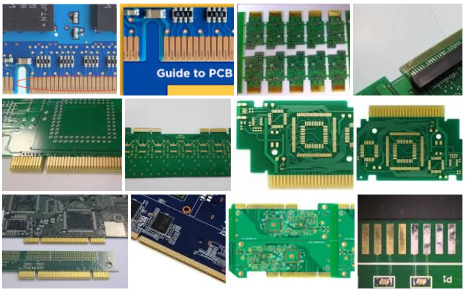
In today's computerized and mobile-activated world, signals are sent between numerous devices. For each command to be enacted, communication must be made between two or more circuit boards. None of this would be possible without gold fingers, which serve as the connecting contacts between motherboards and components like graphics or sound cards.
The technology used to transmit these signals and commands is a huge leap forward from earlier electronics, which typically consisted of separate modules that were difficult to bring into communication with one another. With gold fingers, the processes of one circuit board are immediately read by the main processing board.
The processes associated with this advanced technology extend across all corners of the public and private sectors. In the world of manufacturing, signals are sent between various devices and machines to enact a series of processes, many of which could not be carried out by human hands. At auto-assembly factories and food-packaging plants, numerous commands are fulfilled by computer-prompted machinery, most of which use circuit boards of one size or another.
Many of today`s industrial processes are made possible by gold fingers. So what are they and why are they so important to the inner-workings of computer technology?
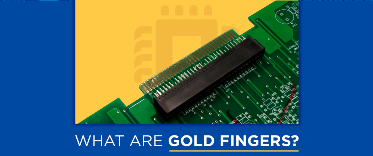
What Are Gold Fingers?
Gold fingers are the gold-plated columns that you see along the connecting edges of Printed Circuit Boards (PCBs). The purpose of gold fingers is to connect a secondary PCB to the motherboard of a computer.
PCB Gold Fingers are also used in various other devices that communicate via digital signals, such as smartphones and smartwatches. Gold is used for the connecting points along a PCB because of the alloy's superior conductivity.
Other names to call a Gold finger PCB abe re a Gold Connector, Edge Connector, Edge-Board Connector, Connector Finger, Contact Fingers, Gold Taps or Gold Tips.
A few of the qualities of the gold fingers include:
- They must be hard in order to allow the circuit board to be inserted into a connector.
- They should also be very smooth and flat to allow for easy insertion.
- They are an excellent conductor which makes the connection much better.
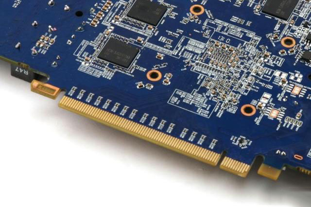
PCB Gold Finger Type
1. Regular golden fingers (flush fingers)
Rectangular pads of the same length and width shall be arranged orderly at the edge of the plate. For example network cards, video cards, etc.
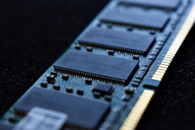
2. Long and short gold fingers (i.e. uneven gold fingers)
A rectangular pad with different length at the edge of the plate. For example memory, U disk, card reader, etc.
3. Segmented golden fingers (interrupted golden fingers)
A rectangular pad with different length at the plate edge and the front section is disconnected
What materials are used to manufacture gold fingers?
Gold fingers are manufactured from flash gold, which is one of the hardest golds around. The specifications to manufacture gold fingers must be precise. Their thickness must be in the range of 3Us to 50Us. Flash gold is used because its high level of harness ensures that it will have a long working life without a need for repair.
Surface Treatment of Gold Finger PCB
1. Nickel gold plating: the thickness can be up to 3-50u ". Due to its superior conductivity, oxidation resistance and wear resistance, it is widely used in the gold finger PCB which needs to be plugged in and out frequently or the PCB which needs to be subject to mechanical friction frequently. However, because of the high cost of gold plating, it is only used in the local gold plating treatment such as gold finger.
2. Immersion Gold: the thickness is 1U in general and 3U in maximum. Because of its excellent conductivity, flatness, and solderability, it is widely used in high-precision PCB boards designed by key position, binding IC, BGA, etc. For the gold finger PCB with low wear resistance requirements, the whole board immersion gold process can also be selected, and the cost of the immersion gold process is much lower than that of the electric gold process. The color of the immersion gold process is golden yellow.
What do gold fingers do?
Used to electroplate the PCB's pads, gold fingers are edge connector contacts. Their function is to assist in protecting the Prototype PCB from deterioration and failures. With the correct thickness and application, gold fingers can be used reliably for close to 1,000 cycles before repair is required.
How are gold fingers applied?
Gold fingers can be used for many different things. Their use would be based on the designer's purpose. Some common applications of gold fingers are:
- Provide an interconnection point for transferring network data.
- A place for attaching daughter boards or specialized adapters.
- Connect external components to the prototype PCB.
- Function as an audio adapter.
How Are Gold Fingers Used?
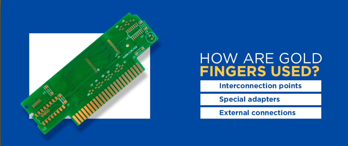
Gold fingers are used as connecting contacts between two adjoining PCBs. Aside from its conductivity, the purpose of the gold is to protect the connecting edges from wear over many uses. Due to the strength of hard gold at its specified thickness, gold fingers make it possible for a PCB to be connected, disconnected and reconnected up to 1,000 different times in a corresponding slot.
The functions of gold fingers are multi-purpose. With any given computer setup, you will see a number of peripherals that connect with the computer itself thanks to PCB gold fingers. Some of the most widespread uses of gold fingers include the following:
Interconnection points: When a secondary PCB connects to the main motherboard, it is done through one of several female slots, such as a PCI, ISA or AGP slot. Through these slots, the gold fingers conduct signals between a peripheral device or an internal card and the computer itself.
Special adapters: Gold fingers make it possible to add numerous performance enhancements to a personal computer. Through secondary PCBs that slot perpendicular into the motherboard, a computer can deliver enhanced graphics and hi-fidelity sound. Since these cards are seldom unattached and reattached, the gold fingers generally outlast the card itself.
External connections: The outer peripherals that have been added to a computer station are connected to the motherboard with PCB gold fingers. Devices such as speakers, subwoofers, scanners, printers and monitors are all plugged into specific slots behind the computer tower. These slots, in turn, attach to PCBs that connect to the motherboard.
The flexibility of the PCB system, whereby different slots connect different types of cards, makes it possible to upgrade the same computer periodically over five or ten years. Every time a sound or graphics card is updated, you can remove the pre-existing card from your motherboard and replace it with the new and improved model. Through each update, the PCB gold fingers remain the universal connecting contact.
Beyond the realm of personal computers, PBC gold fingers are also used as connecting contacts in computerized industrial machinery. The large arsenals of mechanized equipment that you would see at a pressing plant or automotive factory will include an assortment of internal cards that connect to a main source of power via gold fingers. Factory robot arms, for example, are powered with gold finger cards that prompt an assortment of movements.
Why Gold Plaiting Is Necessary For Gold Fingers PCB
Primarily, PCB connection points are subject to constant plugging and unplugging owing to their nature of interconnecting PCBs. Hence, without a strong contact edge, they are prone to wear-and-tear that can cause device malfunctioning. The act of plaiting the connectors with other metals (in this case gold) is done to enhance the durability of the edge connectors.
But I am sure you might have wondered: of all metals, why should edge connectors be gold-plated? Isn`t gold too expensive? Couldn`t copper conduct better and be a lot cheaper than Gold? Well, I have an answer: sure, gold plating of gold fingers is expensive, but it is necessary.
Gold was chosen over other metals because so far, gold has proven to have high corrosion resistance, high electrical conductivity (second to copper and silver) and could be alloyed with cobalt or nickel to increase its resistance to wear-and-tear. Earlier experiments that were done to establish the resistance of gold vis-Ã -vis its resistivity and compared to other popular metals showed that gold had a lower resistance than other metals as shown in Table 1 below.
|
Contact Material |
Resistivity (Ωcm) |
Contact Resistance (mΩ) |
|
Pure Gold |
2.4 X 10⁻⁸ |
0.8 |
|
An alloy of Gold and Cobalt |
2.4 X 10⁻⁸ |
2.6 - 2.8 |
|
Palladium on Nickel |
1.08 X 10⁻⁷ |
3.1 - 5.8 |
|
Silver |
1.6 X 10⁻⁸ |
Non-determined |
Gold is also inert. It does not oxidize or react readily with other metals. This property of gold makes it an ideal choice to make the parts that are prone to be exposed or likely to react with other metals. Even though silver is sometimes useful, it is not recommended for commercial productions as silver is susceptible to sulfide and chloride attacks.
There are two types of gold applicable to the PCB gold finger plating process:
- Electroless Nickel Immersion Gold (ENIG): This gold is more cost-effective and easier to solder than electroplated gold, but its soft, thin (typically 2-5u" composition renders ENIG unsuitable for the abrasive effects of circuit board insertion and removal.
- Electroplated Hard gold: This gold is solid (hard) and thick (typically 30u"), thus more ideal for the abrasive effects of constant PCB usage.
Gold fingers make it possible for different circuit boards to communicate with one another. From the power source to the device or equipment, signals must pass between several contacts for a given command to be enacted.
Once you press a command, the signal will pass between one or more circuit boards before it is read. For example, if you press a remote command on a mobile device, the signal will be sent from the PCB-enabled device in your hand to the near or distant machine, which in turn receives the signal with its own circuit board.
The process involved in the plating of gold fingers involves a number of meticulous steps. This ensures each circuit board rolling off the production line is properly equipped to conduct signals free of error. The standards involved in the plating process also helps to ensure a perfect fit between the gold fingers on each circuit board with the corresponding slots on a given motherboard.
To ensure that all of these fingers and slots fit hand-in-glove, each PCB must pass a series of inspections and defect tests. If the gold plating on a circuit board lacks smoothness or does not adequately adhere to the surface, the results will not be sufficient for commercial release.
For PCB gold fingers to come together, the plating process must be carried out in steps where the surrounding details of the board are completed first. When the time comes to plate the fingers, nickel is applied over the copper. Then, the surface finish is applied last. Once everything has set, the board is inspected under a magnifying lens and subjected to adhesion tests.
Detail Processing of Gold Finger in PCB
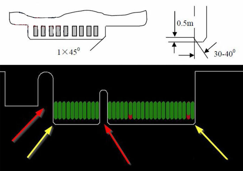
1) to increase the wear resistance of gold fingers, hard gold plating is usually required.2) the golden finger needs to be chamfered, usually 45 °, other angles such as 20 °, 30 °, etc. If there is no chamfer in the design, there is a problem; 45 ° chamfer in PCB is as shown in the following figure:
3) The gold finger needs to be Solder Mask and windowed, and the pin does not need PCB SMT Stencil .
4) The minimum distance between the immersion tin and immersion silver solder pad and the tip of the finger is 14mil. It is suggested that the distance between the solder pad and the finger position should be more than 1mm, including through-hole solder pad;
5) Do not lay copper on the surface of gold fingers;
6) All layers of the inner layer of the gold finger need to be cut copper, which is usually 3mm wide; it can be used for half finger cutting and the whole finger cutting.
Applications & Limitations of Gold Finger PCBs
The uses of PCB gold fingers can be divided into both technical (applications on circuits) and industrial/commercial applications. Let us begin with the Technical application of the contact fingers
Firstly. Technical Applications Of Gold Finger PCBs
Within the circuit, PCB gold fingers have several uses. Some of the technical applications of the connectors are:
- They connect a PCB to a power source: one of the primary uses of the contact fingers is to connect a module PCB to a power source on the connecting profile of a larger PCB.
- They help in the transfer of signals/data: primarily, gold fingers link with the other PCBs to ease the transfer of data and signals between the peripheral PCB and the larger board.
- They interconnect modules within the same board: traditional electronics used to consist of several robust modules that could not be interconnected easily within the same board. With the aid of flexible PCBs electrical engineers were able to interconnect multiple modules even within the same board.
- They provide room for future improvements: well, imagine a computer motherboard without ports and expansion slots. How would it look like? How would it function? And would other interested electricians improve it without adding expansion slots or vendor modules? The picture is unimaginable. You would not be able to connect input devices and output devices. Other engineers would not have worked on the improvement of a computer's keyboard or mouse or VGA card. Simply put: without having gold finger PCBs, machines cannot be improved.
Secondly. Commercial applications
In the industry, gold fingers PCBs are used in several areas. Some of the popular applications include:
- They are used to provide connections for data transfer on network-enabled devices. I.e., we apply Gold fingers in the manufacture of network cards and other additional networking PCB modules.
- They are used to attach specialty adapters. Edge connectors are used to provide an attachment area for special adapters like Video Graphic Array (VGA) cards and other video cards that are useful in processing images. These additional specialized modules relieve the main board some of the processing that is useful when computing.
- They are used to connect other devices to the main processing board. Besides the advantage of connecting network modules and specialized adapters, you can also use gold finger PCBs on the connecting edges of peripheral devices that get connected to the main boards. Their application is relevant in the production of devices like Memory card adapters/readers, flash-drives among other devices. These additional devices can help in boosting processing, adding storage memory or powering the main board.
- They are also used to connect audio adapters to main PCBs.
Regulations, Guidelines & Standards
At the moment, the most popular standards that guide the production of PCB gold fingers are those released by The Institute for Interconnecting and Packaging Electronic Circuits. The organization later transformed into The Association for Connecting Electronics Industries (IPC).
In 2002, IPC released its earliest standards pertaining gold fingers. The IPC-4552 standards of 2002 focused much on guiding the plaiting process of printed circuit boards and PCB finishing. Later, in 2012, they were amended and improved 2012 into the IPC-4556 standards.
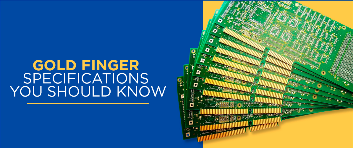
During the PCB gold finger plating process, certain standards must be adhered to for the fingers to function correctly. The design of the PCB itself must also account for the areas needed for proper finger length and alignment. Regardless of the purpose or size of the PCB itself, the following rules are always applicable in the design of gold fingers:
- Plated through holes should never be located close to the gold fingers.
- Gold fingers should not have any contact with solder mask or screen printing, both of which should be kept at a distance.
- Gold fingers must always face the opposite direction from the middle of the PCB (if you want the edge to be beveled)
If any of these rules are not followed during the PCB gold finger plating process, the PCB might be incapable of communicating with the parent circuit board. Alternately, the PCB might not fit properly into the appropriate slot on a motherboard.
The reason why gold is used for the connecting fingers on PCBs is due to the alloy`s superior strength and conductivity. The strength of gold makes it possible for the fingers to be inserted and ejected hundreds of times without wear to the connecting contacts. Without the protection of the gold plating, a circuit board could easily be stripped of its connecting functions after a few uses.
You might wonder why gold over other types of metal. After all, gold is one of the rarest and most expensive natural elements. Might it be more cost-effective to plate the connecting edges of PCBs with copper or nickel? Gold, however, is necessary for the functions required of a Printed Circuit Board.
As PCBs were developed into their modern-day form, gold was identified as the most suitable connecting-contact metal on account of several factors. The main benefits of gold are the alloy`s electrical conductivity and resistance to corrosion. For added strength, the gold used in printed circuit boards is usually alloyed in combination with nickel or cobalt, which lend the gold further resistance to wear in the face of constant PCB activity. For the plating process, the nickel has a thickness of between 150 and 200 microinches.
In 2015, the standards were again amended with the release of IPC A-600 and IPC-6010, which are currently the most widely employed standards in PCB production. The IPC standards can be summarized as follows:
Chemical composition: For maximum rigidity along the edges of PCB contacts, the gold plating should consist of between 5 and 10 percent cobalt.
PCB Gold Fingers Thickness: The plating thickness of gold fingers should always fall within the range of 2 to 50 microinches. The standard thicknesses by size are 0.031 inches, 0.062 inches, 0.093 inches and 0.125 inches. The lower thicknesses are generally used for prototypes while the higher thicknesses are used along connecting edges that are regularly inserted, unplugged and reinserted.
Visual test: Gold fingers should pass a visual test conducted with a magnifying lens. The edges should have a smooth, clean surface and be free of excess plating or the appearance of nickel.
Tape test: To test the adhesiveness of the gold plating along the contacts, the ICP recommends a test whereby a strip of tape is placed along the contact edges. After removing the tape, inspect the strip for traces of plating. If any gold plating is evident on the tape, the plating lacks sufficient adhesiveness along the contacts.
Numerous other standards exist for the PCB gold finger plating process, and all should be read in full for an in-depth understanding. As technology improves, further standards of testing are commonly introduced to the process, so it is best to check back with the IPC for updates periodically.
What is PCB Gold Finger Window
What is the PCB window? Generally speaking, the wires on PCB are covered with oil to prevent short circuits. The window opening is to remove the paint layer on the wires so that the wires are exposed and easy to tin, that is to say, the purpose of "copper exposure" is not separated by anti soldering ink.The most common PCB window opening is seen in the gold finger, which is the electrical connection pin between PCB and other equipment such as mainboard, chassis, etc. it is used for "plugging" in products. Because a thin layer of gold is plated on the nickel plating layer of copper foil, the English "binding finger", it is called "gold finger". We are familiar with the computer memory module and have a golden finger structure. People who have disassembled the computer know that the memory module has a golden finger on one side, and the golden finger on it is to open a window, plug, and play.
In general PCB Manufacturing process, the gold finger is made by "opening window", that is, there is no anti welding (green paint) between its pads, so as to avoid the anti welding falling off caused by long-term plugging and plugging, which will affect the quality of the product itself. In addition, window opening has a common function, which can increase the thickness of copper foil in the later stage of tin ironing to facilitate excessive current, which is more common in the power board and motor control board.
How to realize the PCB window? Take Altium designer 10 for example, if you want to open a window on the top layer, you only need to place the same line as the wire on the top solver layer. Similarly, if you want to open a window on the bottom layer, you only need to place the line on the bottom layer.
But there are exceptions. If it is a general SMD (one of the SMT components), it is necessary to avoid this problem. In PCB layout design, pad spacing should be increased or pad size should be reduced. However, because the PCB media layer itself has the property of non-tin affinity, it has the ability to block the bridge originally, so in principle, it will not cause short circuit problems.
PCB Gold Finger Beveling
On a circuit board, the PCB gold finger plating process is used after the solder mask and before the surface finish. The plating process generally consists of the following steps:
Nickel plating: Between three and six microns of nickel are plated first to the connector edges of the fingers.
Gold plating: Between one and two microns of hard gold are plated over the nickel. The gold is usually enhanced with cobalt for boosted surface resistance.
Beveling: The connector edges are beveled at specified angles for easier insertion on corresponding slots. Beveling is typically done at angles of 30 to 45 degrees.
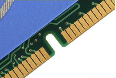
On some circuit boards, certain gold fingers will be longer or shorter than others. For example, a circuit board may have longer fingers at one end. This way, the PCB is easier to insert into a slot, as the end with the longer fingers will snap into place more readily. From there, you simply push the other end of the PCB into place.
There are certain restrictions to the plating process. For example, certain distances are needed between the gold fingers and other parts of the circuit board. Key restrictions include the following:
- Inner layers must be copper-free along the PCB edge to prevent copper exposure during the beveling stage.
- Plated holes, SMD and pads should not be placed within 1.0 millimeters of the gold fingers.
- Plated pads cannot exceed 40 millimeters in length.
- A distance of 0.5 millimeters should exist between the gold fingers and the outline.
Any deviation from the standard spacing requirements around the gold fingers on a printed circuit board could result in a physically weak or dysfunctional card.
Limitations of Gold Finger PCB Technology
Even though gold finger technology is of great importance, its application is still limited in that:
- Plated pads must be on the edge of a PCB. Because gold plating involves an electroplating process, there must be a connection linking the plated pads with the connections panel frame.
- Most plating pads are limited to produce gold fingers that do not stretch over 40mm. In case you might need to have longer gold fingers, the process of manufacturing them might increase.
- Inner layers of the edge connectors have to be free of copper. Otherwise, the process of beveling the contacts might expose the copper.
- Except for flexible PCBs, when plating on both sides of a PCB, the minimum separating distance between the upper and the lower layers of the PCB is supposed to be 150mm.
How Gold Fingers Are Changing the World
Today's computer and mobile devices are growing ever-more complex as manufacturers compete to make their products faster and more resourceful. If you build a large computer station and amass a handful of mobile devices, you are liable to have numerous gold-plated circuit boards interacting at the same time. Each time you print out an article or scan a photo to upload to a social media account, signals are sent from peripheral devices to motherboard cards, which receive these signals via PCBs.
Thanks in large part to gold fingers, technology has been able to advance to the modern array of mobile devices that millions now use on a daily basis. Moreover, gold fingers have allowed industries to become more productive and capable than ever before.
As increasing amounts of technology rely on gold fingers, it is crucial to have them plated and tested to the highest standards. Only this way can you ensure maximum performance without fail from the tech products that use circuit boards. At JingHongYi PCB (HK) Co., Limited, we provide PCBs of the highest quality for customers in a variety of industries. Contact us today for a free quote.
Is the "gold" of Gold Finger Gold?
First, we need to understand two concepts: soft gold and hard gold. Soft gold, generally gold. Hard gold, usually a compound of hard gold.
The main function of the gold finger is connection, so it must have good conductivity, wear resistance, oxidation resistance and corrosion resistance.
Due to the soft texture of pure gold (gold), gold fingers generally do not use gold, but only electroplate a layer of "hard gold (gold compound)" on it, which can not only obtain good conductivity of gold but also make it have wear resistance and oxidation resistance.
Has PCB ever used "soft gold"? The answer, of course, is used, such as the contact surface of some mobile phone buttons, aluminum wire on the cob (chip on board), etc. The soft gold is usually deposited on the circuit board by electroplating. Its thickness control is more elastic.
Tip: no matter whether the PCB is plated with soft gold or hard gold, the amount will not be too much. Please don't dismantle the electronic instrument for "taking gold"!
Gold Fingers PCB Manufacturer in China
Jinghongyi PCB is a professional manufacturer of PCB. In the past 10 years, it has focused on the prototype and batch production and assembly of single-sided, double-sided and multi-layer PCB. It can provide multi-layer PCB prototypes such as impedance PCB and blind buried PCB, and large, medium and small batch production business of PCB.
Whatever you need - we can provide it.
We help start-ups to provide Quick Turn PCB fabric services, while meeting the growing sales demand of enterprises, providing high-quality products for all industries. With our strong expertise, capabilities, and relationships with many upstream and downstream suppliers, we can provide fast turnaround delivery, mass production and effectively handle all technical and quantity requirements within a few working days.
Our company has its own factory for direct production without any outsourcing. The company is headquartered in Shenzhen, China. There is a complete PCB industrial chain around the factory. In addition, we have very good cooperation with raw material suppliers and logistics companies, which can ensure the supply of raw materials and the timely and accurate delivery of products to your hands after the completion of production.
If you have the following problems, you should consider changing suppliers:
1. Suppliers' quotation is needed, but they haven't replied for a long time
2. Suppliers always shirk responsibility for product quality problems
3. Contact the customer service personnel or engineer of the supplier, the response speed is very slow or there is no reply
4. The supplier's cooperation is not enough, which always makes you confused
It's not a problem with us. We use the modern management concept to ensure the good communication and connection of each link. It's not our goal to satisfy our customers. Our goal is to exceed the expectations of our customers. Please believe us, we are your best choice.
Gold Fingers PCB
Gold Fingers PCB, Gold Fingers Circuit Board, PCB Gold Fingers
JingHongYi PCB (HK) Co., Limited , https://www.pcbjhy.com
