Introduction to the development and manufacturing process of microfluidic chips
The concept of the micro-total analysis system was first proposed by Manz and Widmer of Ciba2Geigy in Switzerland in 1990. At that time, it mainly emphasized the "micro" and "full" of the analysis system, and the MEMS processing method of the micro-pipe network. Clarify its appearance characteristics. The following year, Manz et al. realized capillary electrophoresis and flow on a flat microchip. The current development frontier of the micro total analysis system. The microfluidic analysis system has developed from capillary electrophoresis separation as the core analysis technology to liquid-liquid extraction, filtration, membraneless diffusion and other separation methods. Among them, the multiphase laminar flow separation microfluidic system has a simple structure, has a variety of separation functions, and has a wide range of application prospects. There have been many reports in the literature on the use of multiphase laminar flow technology to achieve membraneless filtration, membraneless analysis and extraction and separation of samples on the chip. At the same time, there are also reports on the use of micro-machined membrane microdialyzers to complete the sample pretreatment operations before mass spectrometry analysis. The fluid control analysis system has developed from electro-osmotic flow as the main liquid flow driving method to hydrodynamic pressure, heavy motion, centrifugal force, shear force and other methods.
Until today, scientists from various countries have made more remarkable achievements in this field. As an important development frontier of current analytical science, microfluidic technology has achieved rapid development in both research and application.
Principle of microfluidic chip

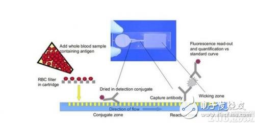
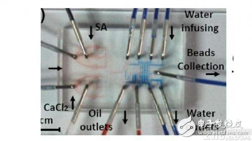
The microfluidic chip uses a semiconductor-like microelectromechanical processing technology to construct a microfluidic system on the chip, and transfers the experiment and analysis process to the chip structure composed of interconnected paths and liquid phase chambers. After loading biological samples and reaction liquids , Using micro-mechanical pumps. Methods such as electric hydraulic pump and electroosmotic flow drive the flow of the buffer in the chip to form a micro flow path, and one or more continuous reactions are performed on the chip. A variety of detection systems such as laser-induced fluorescence, electrochemistry, and chemistry, as well as many detection methods combined with analysis methods such as mass spectrometry, have been used in microfluidic chips to perform rapid, accurate and high-throughput analysis of samples. The biggest feature of a microfluidic chip is that a multi-functional integrated system and a large number of composite systems can be formed on a single chip for a micro total analysis system? Microreactors are commonly used structures for biochemical reactions in labs on a chip, such as microreactors for capillary electrophoresis, polymerase chain reaction, enzyme reactions, and DNA hybridization reactions. Among them, voltage-driven capillary electrophoresis (Capillary Electrophoresis, CE) is relatively easy to implement on a microfluidic chip, and thus has become the fastest-growing technology among them. It is to etch the capillary channel on the chip, and the sample liquid moves in the channel under the action of electroosmotic flow to complete the detection and analysis of the sample. If the capillary array is built on the chip, hundreds of samples can be completed in a few minutes. Parallel analysis. Since the first report of the microfluidic chip CE in 1992, has it progressed rapidly? The first commercial instrument is the microfluidic chip CE (Biochemical Analyzer, Aglient), which can provide microfluidic chip products for nucleic acid and protein analysis.
Features of microfluidic chipThere are more and more unit components integrated in the chip, and the scale of integration is returning larger, so that the microfluidic chip has a strong integration. At the same time, a large number of samples can be processed in parallel, which has the characteristics of high throughput, fast analysis speed, low consumption, low material consumption, and low pollution. The amount of reagents required to analyze samples is only a few microliters to dozens of microliters, which is only a few microliters to dozens of microliters. The volume is even upgraded in nano or leather.
Cheap and safe, therefore, the microfluidic analysis system is miniaturized. The advantages of integrated chemical integration and portability provide extremely broad prospects for its application in many fields such as biomedical research, drug synthesis screening, environmental monitoring and protection, health quarantine, judicial identification, and biological reagent testing.

1. Lithography and etching
1. Lithography
Lithography is micro-manufacturing using photoresist, mask and ultraviolet light. The process is as follows:
â‘ Wash the substrate carefully;
â‘¡Plating a barrier layer on the surface of the clean substrate, such as chromium, silicon dioxide, silicon nitride, etc.;
â‘¢Use a glue spinner to evenly spin a layer of photosensitive material with a thickness of several hundred A-photoresist on the barrier layer. The actual thickness of the photoresist is related to its viscosity and is inversely proportional to the square root of the spinning speed of the spinner;
â‘£Prepare the required channel pattern on the photomask. Cover the photomask on the substrate, irradiate the substrate coated with photoresist with ultraviolet light, and the photoresist undergoes a photochemical reaction;
⑤The exposed photoresist is removed by the chemical method of development with the photoresist supporting developer. In this way, the two-dimensional geometric pattern on the film can be accurately copied to the photoresist layer by the method of plate making;
â‘¥ After drying, the protective effect of the unexposed photoresist is used to precisely etch the planar two-dimensional pattern on the negative film on the barrier layer by a chemical etching method.
2. Mask preparation
When processing microfluidic chips by photolithography, a photolithography mask must be manufactured first. The following requirements are imposed on the mask:
①The contrast between the patterned area and the non-patterned area of ​​the mask for light absorption or transmission should be as large as possible;
â‘¡The defects of the mask, such as pinholes, broken bars, bridges, dirty spots, and uneven lines, should be as few as possible;
â‘¢The pattern precision of the mask should be high.
The photolithography mask materials commonly used for large-scale integrated circuits are chrome-plated glass plates or quartz plates coated with photoresist. The computer graphics system is used to convert the mask pattern into a data file, and then the exploding light source, iris diaphragm, worktable and lens in the pattern generator are controlled through a dedicated interface circuit, and the required pattern is carved on the mask material. However, due to the expensive equipment, general domestic scientific research units have to solve the problem through outsourcing, which delays the research cycle.
Since the resolution of the microfluidic chip is much lower than the requirement of large-scale integrated circuits, it has recently been reported that a simple method and equipment are used to prepare a mask. After the structure diagram of the designed microchannel is converted into an image file by a computer through CAD software, A high-resolution printer is used to print the image on a transparent film. The transparent film can be used as a mask for photolithography, which can basically meet the requirements of the microfluidic analysis chip for the mask.
Earth auger are used in both temporary or permanent applications, including supporting retaining walls,guyed masts, and circus tents.garden or vineyard fence & .
Helical Ground anchor mainly made of carbon steel/ thread steel ,with high dip galvanized surface treatment or powder coated treatment .
There are many colors of ground anchor ,such as black ,white ,red colors .
diameter of ground anchor pole :13-16 mm,length 30-60' or according to clients' request .
In addition to earth anchor,we also supply earth auger,helical Ground Screw anchor,helical ground anchor,ground anchor pile,anchor Bolt.
Earth Auger,Anchor,Pile Anchor,Earth Screw
BAODING JIMAOTONG IMPORT AND EXPORT CO., LTD , https://www.chinagroundscrew.com
