The long-term benefits of solid-state lighting (SSL) are clear: lower energy costs, longer life, better illumination and greater flexibility. However, due to the high cost, it cannot be applied on a large scale. Therefore, it is imperative to seek a solution to reduce costs.
[Source: "High - tech LED - Technology and Applications " 1 February issue ]
A key factor in significantly reducing costs is the use of large dimensions, such as 150 mm (6 in.) or larger substrate sheets to make LED chips. The silicon industry achieved this transition 20 years ago and has also led to advances in automation control and traceability. The advantages of large-sized substrate sheets will be further explored below.
Traditional sapphire growth techniques have encountered significant obstacles in growing large-sized substrates. The inevitable serious defects of a growth technology reduce the overall material utilization. In addition, substrates made using conventional sapphire growth techniques have stress and strain variations that can cause severe bow and warpage problems in LED fabrication.
Advantages of large size substrate
We believe that one of the key factors in reducing the price of high-brightness LED chips is the use of large-sized substrates. Large size substrates can make more chips in each MOCVD run.
In general, for every 50 mm increase in substrate diameter, there will be a significant increase in substrate surface area. For example, the surface area of ​​a substrate having a diameter of 150 mm is 9 times that of a substrate having a diameter of 50 mm (actual diameter of 50.8 mm). However, as the surface area of ​​the substrate increases, the area of ​​the "edge exclusion zone" also increases, but the increase is small. The results show that the actual surface area of ​​the 150 mm diameter substrate is 10.3 times that of the 50 mm diameter substrate.
LED chip dicing simulation makes the advantages of large-size substrates more obvious. We simulated the dicing of the 45*45mil chip commonly used for high-brightness LEDs. As shown in Figure 1, the chips labeled red are not in the statistical range because they are chips that fall within or border the "edge exclusion zone" (3mm area indicated by the yellow dashed line). Chips (shown in black areas) that fall outside the substrate are also not in the statistical range.
Due to the larger size of the substrate, which is equivalent to the grid of LED chips, there is less edge exclusion zone curvature, and fewer chips are lost per unit surface area. There is a growing trend in the industry to use large-sized chips to improve lumens per watt performance, and if small-sized substrates are used, more chips are lost per unit surface area.
Figure 2 summarizes the total surface area, the comparison of the efficiency and relative curvature of the edge exclusion zone. As shown in Figure 2, the number of chips obtained for a 150 mm diameter substrate is 10.9 times that of a 50 mm diameter substrate (the simulated chip size is 45 x 45 mils). The number of chips obtained for a 200 mm diameter substrate was 19.8 times that of a 50 mm diameter substrate. These advantages determine that more LED chips can be produced in each round of MOCVD equipment production.
We observed the performance and advantages of these large-sized substrates in MOCVD reactors. Compared with processing large-size substrates, the reactor can process more small-sized substrates at the same time. Therefore, considering the advantages of large-size substrates, it is also necessary to consider these. factor.
The MOCVD growth phase is the most expensive part of the entire LED production process. Each round of MOCVD growth can carry many small size substrates. Even so, the use of a small number of large-sized substrates ultimately yields more chips than smaller-sized substrates. Let us first look at the layout of the 50mm, 150mm and 200mm substrates in MOCVD.
Unfinished
For more information, please refer to "High - tech LED - Technology and Applications" 1 February issue
Simulations show that the increase in surface area and chip count is significant. For a 150 mm diameter substrate, MOCVD can increase the yield of 55% of the chip, and the advantage of a 200 mm diameter substrate is greater. A recent study, shown in the US Department of Energy report, also yielded a similar conclusion that a 150 mm diameter substrate can achieve 52% more chips than a 50 mm diameter substrate. The long-term benefits of state of the art (SSL) are clear: lower energy costs, longer life, better illumination and greater flexibility. However, due to the high cost, it cannot be applied on a large scale. Therefore, it is imperative to seek a solution to reduce costs.
A key factor in significantly reducing costs is the use of large dimensions, such as 150 mm (6 in.) or larger substrate sheets to make LED chips. The silicon industry achieved this transition 20 years ago and has also led to advances in automation control and traceability. The advantages of large-sized substrate sheets will be further explored below.
Traditional sapphire growth techniques have encountered significant obstacles in growing large-sized substrates. The inevitable serious defects of a growth technology reduce the overall material utilization. In addition, substrates made using conventional sapphire growth techniques have stress and strain variations that can cause severe bow and warpage problems in LED fabrication.
Advantages of large size substrate
We believe that one of the key factors in reducing the price of high-brightness LED chips is the use of large-sized substrates. Large size substrates can make more chips in each MOCVD run.
In general, for every 50 mm increase in substrate diameter, there will be a significant increase in substrate surface area. For example, the surface area of ​​a substrate having a diameter of 150 mm is 9 times that of a substrate having a diameter of 50 mm (actual diameter of 50.8 mm). However, as the surface area of ​​the substrate increases, the area of ​​the "edge exclusion zone" also increases, but the increase is small. The results show that the actual surface area of ​​the 150 mm diameter substrate is 10.3 times that of the 50 mm diameter substrate.
LED chip dicing simulation makes the advantages of large-size substrates more obvious. We simulated the dicing of the 45*45mil chip commonly used for high-brightness LEDs. As shown in Figure 1, the chips labeled red are not in the statistical range because they are chips that fall within or border the "edge exclusion zone" (3mm area indicated by the yellow dashed line). Chips (shown in black areas) that fall outside the substrate are also not in the statistical range.
Due to the larger size of the substrate, which is equivalent to the grid of LED chips, there is less edge exclusion zone curvature, and fewer chips are lost per unit surface area. There is a growing trend in the industry to use large-sized chips to improve lumens per watt performance, and if small-sized substrates are used, more chips are lost per unit surface area.
Figure 2 summarizes the total surface area, the comparison of the efficiency and relative curvature of the edge exclusion zone. As shown in Figure 2, the number of chips obtained for a 150 mm diameter substrate is 10.9 times that of a 50 mm diameter substrate (the simulated chip size is 45 x 45 mils). The number of chips obtained for a 200 mm diameter substrate was 19.8 times that of a 50 mm diameter substrate. These advantages determine that more LED chips can be produced in each round of MOCVD equipment production.
We observed the performance and advantages of these large-sized substrates in MOCVD reactors. Compared with processing large-size substrates, the reactor can process more small-sized substrates at the same time. Therefore, considering the advantages of large-size substrates, it is also necessary to consider these. factor.
The MOCVD growth phase is the most expensive part of the entire LED production process. Each round of MOCVD growth can carry many small size substrates. Even so, the use of a small number of large-sized substrates ultimately yields more chips than smaller-sized substrates. Let us first look at the layout of the 50mm, 150mm and 200mm substrates in MOCVD.
Figure 3 shows the layout of three common substrates within the MOCVD reactor, including large and small substrates. It can be seen that the surface area (red portion) of the single-piece 150 mm substrate is larger than 7 substrates having a diameter of 50 mm. This chart shows that a larger substrate can achieve a relatively higher yield.
Simulations show that the increase in surface area and chip count is significant. For a 150 mm diameter substrate, MOCVD can increase the yield of 55% of the chip, and the advantage of a 200 mm diameter substrate is greater. A recent study, shown in the US Department of Energy report, also yielded a similar conclusion that a 150 mm diameter substrate can achieve 52% more chips than a 50 mm diameter substrate.

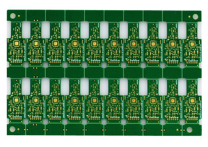
4-layer Medical Treatment PCB Board, Base Material: FR4 TG135. inner/outer copper thickness 1/1.5 oz. Immersion Gold 3U" surface finished. With green colour solder mask and white silkscreen. Board thickness 1.0 mm. Min.line width/Min.line spacing 0.12/0.15 mm. 20-up connect with the routed&v-cut, 100% E-test pass. there are Vias in pad need to be filled with resin and copper cap. Outline Profile tolerance +/-0.1 mm. line width / distance tolerance +/-15%. hole copper 30 um.The medical treatment PCB boards are usually of high precision, strict control of various tolerances required

Medical Treatment PCB Board
Medical Treatment PCB Board,Medical Treatment PCB Panel,Medical Treatment Circuit Board,Circuit Board Etching
Orilind Limited Company , https://www.orilind.com


