LED driver low noise constant current charge pump error amplifier EA design
Modern portable digital devices are inseparable from displays, and white LEDs (light-emitting diodes), which are backlights for displays, are many times better than traditional CCFLs (Cold Cathode Fluorescent Lamps) in many respects (such as service life and energy consumption). Even dozens of performances, so it has become a trend by it as a display backlight.
Since the brightness of white LEDs is greatly affected by their driving current, it is always a hotspot to design a stable current driver. One of the methods is to use a series connection LED method, which is complicated in structure and requires inductance. It will generate EMI and occupy a large chip area and high cost. The other way is to use a charge pump to provide several constant currents in parallel. This method does not require inductance, so there is no such problem as EMI in the first way. The EA described herein is an LED driver for such a charge pump that ensures a constant charging current for low noise operation.
EA is a basic integrated circuit (IC) analog circuit unit with its high precision voltage reference, low noise, high power supply noise rejection ratio (PSRR) and high common mode rejection ratio (CMRR). It is widely used in analog-to-digital converter ADCs, digital-to-analog converter DACs, LDO drivers, and RF circuits. A new EA for charge pump is designed in this paper. Compared with the EA that appeared before, the characteristics of the EA are as follows:
1) The input stage power supply of the error amplifier is biased by the stable output of the charge pump instead of continuously decreasing, thereby ensuring the stability of the power supply;
2) Introducing a dynamic compensation circuit to ensure frequency characteristics while reducing cost; the traditional method is to use external capacitors and their equivalent series resistors for frequency compensation;
3) The Maitreya capacitor in the capacitor not only compensates for the frequency, but also further improves the PSRR performance of the circuit;
4) Some additional circuits, such as start-up circuit, load current sampling, overcurrent protection, etc., can further improve the accuracy of the entire circuit.
1 circuit designThe circuit of the improved error amplifier and some additional circuits and feedback circuits are shown in FIG. 1. For the convenience of analysis, each functional module is drawn by a broken line in the figure.
1.1 error amplifierThe core of this circuit is a high gain large PSRR transconductance operational amplifier (OTA), the other includes a primary amplifier Gml, a secondary amplifier Gin2, and a frequency compensation circuit. Where Gml is the basic symmetric OTA of the differential input, it amplifies the reference voltage and VOUT divided signal fed back from the positive and negative terminals respectively. The bias current module consists of M7, M8, M11, M12, M13, M14, M15 and R3. The bias current I0 is twice that of I3, and is set by the reference voltage Vref, the threshold voltage of the NMOS transistor M15, and R3. The source terminals of M7 and M8 are connected to the output of the charge pump VOUT, so the error amplifier can be operated when VOUT reaches a certain value (such as 3.6 V) by setting M7 and M8. At the same time, this part also generates an SN signal to activate the overcurrent protection unit and provide bias. The output stage of Gm1 is a current amplification structure consisting of M3, M6, M9 and M10 with an amplification ratio of 3:1, ie: (W/L)6:(W/L) 5=(W/L)4: (W/L) 3 = 3: 1, where W and L are the width and length of the transistor, respectively. This ratio is obtained after a compromise between gain bandwidth, phase margin, and output noise.
The gain Gm2 of the second stage amplifying circuit is mainly used to increase the open loop gain of the circuit and reduce the output impedance of the error amplifier, thereby increasing the bandwidth. It is an inverting amplifier consisting of M20 and M21. Both tubes have a large aspect ratio. The aspect ratio of M16 and M20 in the frequency compensation circuit determines the low frequency open loop gain of the circuit.
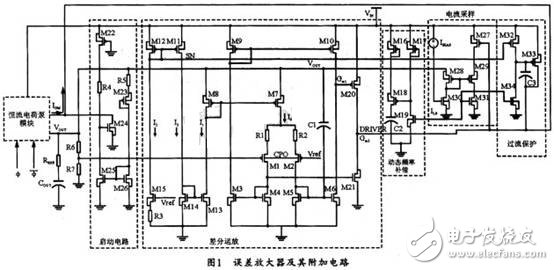
In order to improve the frequency characteristics of the circuit, two compensation circuits are used in this design. One is a dynamic frequency compensation circuit, such as the RC network consisting of a switching resistor and a MOS transistor parasitic capacitor, as shown in Figure 1, which can change the operating point of the MOS transistor by sampling the load current, ie by changing the switching resistance and MOS tube parasitics. The value of the capacitor is used to achieve dynamic compensation. Since the zero-pole frequency increases (decreases) as the load current increases (decreases), the charge pump unity gain frequency (UGF) remains essentially constant as the load changes, which ensures that the charge pump is fully loaded. Stable work within the scope. The dynamic frequency compensation circuit in Fig. 1 includes M16, M17, M18, M19 and C2, wherein M16, M18 and C2 are not only the load of the amplifier Gml, but also the function of frequency compensation. Here, the gate area of ​​the M18 is designed to be large to generate a large parasitic capacitance. M31 and M19 in the current sampling circuit form a mirror current source, and their W/L ratio is designed to be 1:5. According to the basic principle of transistor operation, the gate voltage VGM18 of M18 is:
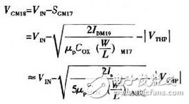
From the above equation, the relationship between VGM18 and IS (sampling current, here IS≈IGM/3000) can be clearly seen, that is, VGM18 varies with IGM. That is to say, the RC dynamic compensation network will change with the change of IGM.
Another frequency compensation in the circuit uses the capacitance C1 between the first and second stage amplifiers, and feedback is introduced from the output, which simultaneously increases the PSRR of the circuit.
1.2 Other function modulesIn addition, when designing this circuit, some other functional modules should be designed, including: start circuit, current sampling, over current protection and other circuits.
Unlike the traditional method, this design connects the power supply bias of the Gml differential input to the output voltage VOUT of the charge pump instead of VIN, which makes the bias voltage very stable, because the ripple of VOUT is small, and The noise is extremely low.
However, this design also has a problem: VOUT is zero at the beginning of the system power-on, and the EA does not work at this time, making the entire circuit inoperable. Therefore, it is necessary to add a boot unit to make the system just At power-up, the charge pump can be operated, causing VOUT to rise, and when VOUT increases to a threshold, EA begins to operate. When the circuit is activated, the charge pump drive voltage is enabled by the EA output controls M22, R4, and M24 to turn the circuit on, while M23, M25, M26, and R5 turn it off.
The current sampling circuit in the system takes a small current IS proportional to the IGM, which consists of M27, M28, M29 and M30. The gate of M27 should be connected to the gate of the current mirror in the charge pump to set the sampling ratio to 1:3000. The sampling principle is as follows:
Since the reference circuit provides a very small bias current (approximately 1μA), the gate-source voltage VGS of the M28 is small, almost the threshold voltage. While the width/length ratio W/L of the M29 is designed to be large, the sampling current IS is small, and the gate-source voltage VGS of the M29 is also small. Therefore, the M27 and the VDRAIN of the switching tube in the charge pump are almost the same size. Its overcurrent protection circuit includes M32, M33 and M34. Here, M34 and M31 of the current sampling circuit are mirror images of each other. It controls the gate voltage of the switching transistor in the charge pump by sampling the current IS, thus limiting the maximum value. In the normal range, IS is small, M32 and M34 are driven together, M33's VGATE is high, and the overcurrent protection unit does not work. As the IGM increases, the VDRAIN of M34 (or the VGATE of M33) will slowly decrease. When increased to a certain value, M33 is fully turned on, and the feedback loop limits VDRIVER to a certain value, thereby limiting the IGM and implementing overcurrent protection. The dimensions of the M32, M33 and M34 should be matched to the design. During current limiting operation, the circuit forms a feedback loop and C3 acts as a Maitreya compensation to stabilize the defined current.
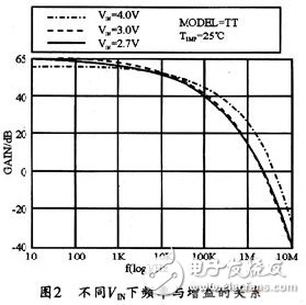
2 simulation resultsTo evaluate the performance of the designed circuit, the system was simulated using the Hynix 0.5μm CMOS process. Figure 2 shows the comparison of the frequency and gain of the HSPICE simulation at different supply voltages. The simulation results show that it is in a wide frequency range. The gain is over 60 dB.
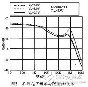
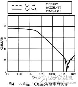
The relationship between PSRR and frequency at different supply voltages and the relationship between CMRR and frequency at different IGMs are given in Figures 3 and 4, respectively. The results show that the circuit's PSRR and CMRR can reach 65 dB and 70 dB, respectively.
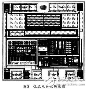
To further determine the usability of the design, a constant current charge pump layout using the EA is also drawn here, as shown in Figure 5, for subsequent work.
Based on the symmetrical OTA structure, this paper designs an error amplifier EA for low noise constant current charge pump, which introduces dynamic frequency compensation and Maitreya compensation based on the traditional design. The newly designed EA not only reduces output ripple and noise, but also improves stability. From the circuit analysis and simulation results, it can be seen that the gain is as high as 60 dB, the PSRR is 65 dB, and the CMRR is as high as 70 dB in the frequency range of 100 Hz to 10 MHz, and the system achieves high performance.
Langrui Energy (Shenzhen) Co.,Ltd , https://www.langruibattery.com
