
PCB board design must see common sense! What is the difference between single-layer FPC/double-sided FPC/multi-layer FPC, self-learning materials
Although the engineers of the circuit board factory do not participate in the design of the circuit board, but the original design data of the customer is made into the PCB circuit board production materials inside the company, but through years of practical experience, the engineers have already designed the PCB circuit board. Accumulation, summarized as follows for reference only:
1. If the FPGA system is designed to include the FPGA device, the pin assignment must be verified using the Quartus II software before drawing the schematic. (Some special pins in the FPGA cannot be used as normal IO).
From the top to the bottom of the 2.4-layer circuit board are: signal plane layer, ground, power supply, signal plane layer; 6-layer circuit board from top to bottom are: signal plane layer, ground, signal inner layer, signal inner layer, Power supply, signal plane layer. More than 6 layers (the advantage is: anti-interference radiation), the inner layer is preferentially selected, the plane layer is not selected, and the ground or power layer is prohibited from being routed (cause: the power layer will be split and parasitic effects will be generated).
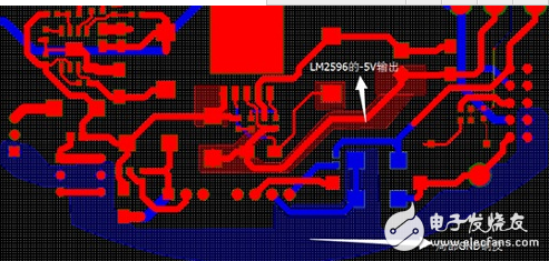
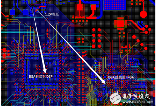
3. Multi-power system wiring: If the FPGA+DSP system is a 6-layer circuit board, it will generally have at least 3.3V+1.2V+1.8V+5V.
3.3V is generally the main power supply, directly paving the power layer, and it is easy to pass through the global power network through the vias;
5V is generally a power input and only needs to be copper in a small area. And as thick as possible (you ask me how thick it is - how thick it is, how thick it is, the thicker the better);
1.2V and 1.8V are core power supplies (if direct connection is used, it will be very difficult to face BGA devices). When layout, try to separate 1.2V from 1.8V and connect it to 1.2V or 1.8V. The components are arranged in a compact area, connected by copper, as shown in the figure:
In short, because the power network is spread over the entire PCB board, if the way of routing is complicated and will go very far, the method of using copper plating is a good choice!
4. Cross-connection between adjacent layers: It can reduce the electromagnetic interference between parallel wires (high school), and it is convenient for routing.
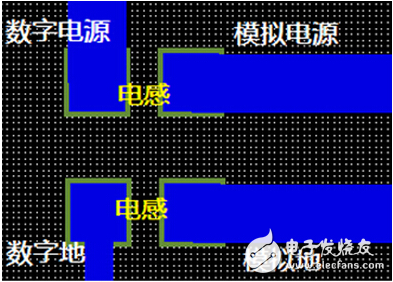
5. Analog numbers should be isolated, how is it isolated? The device that separates the analog signal is separated from the digital signal device in the layout, and then cuts from the middle of the AD chip!
The analog signal is grounded analog, and the analog ground/analog power supply is connected to the digital power supply through a single point of the inductor/bead.
6. PCB circuit board design based on PCB design software can also be regarded as a software development process. Software engineering pays most attention to the idea of ​​“iteration developmentâ€. I think this idea can also be introduced in PCB design to reduce the probability of PCB errors.
(1) Schematic inspection, paying particular attention to the power supply and ground of the device (the power supply and the ground are the blood vessels of the system, and there must be no negligence);
(2) PCB package drawing (confirm whether the pins in the schematic are incorrect);
(3) After confirming the PCB package size one by one, add a verification label and add it to the design package library;
(4) Import the netlist and adjust the signal sequence in the schematic while layout (the automatic auto-numbering function of OrCAD can no longer be used after layout);
(5) Manual wiring (check the power supply network on the side of the cloth. As mentioned earlier: the power supply network uses copper plating, so use less wiring);
In short, the guiding idea in PCB design is to draw the package schematic layout feedback correction schematic (from the correctness of the signal connection, the convenience of signal routing).
7. The crystal oscillator is as close as possible to the chip, and the crystal oscillator should not be routed as much as possible. The clocks used in multiple places are routed using a tree clock tree.
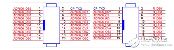
8. The arrangement of the signals on the connector has a great influence on the ease of wiring. Therefore, adjust the signal on the schematic while wiring (but never renumber the components).
9. Multi-board connector design:
(1) Use the cable connection: the upper and lower interfaces are consistent;
(2) Straight socket: The upper and lower interfaces are mirror-symmetrical, as shown below:
10. Module connection signal design:
(1) If two modules are placed on the same side of the PCB, the discipline number is larger than the small one (mirror connection signal);
(2) If two modules are placed on different sides of the PCB, the discipline number is small and large.
This allows the signal to be placed as if it were crossed as shown on the right. Of course, the above method is not a rule. I always say that everything changes with the needs (this can only be understood by myself), but in many cases, designing in this way is very useful.
11. Power ground loop design:
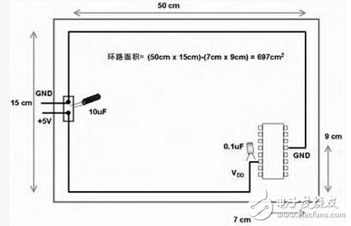
The power ground circuit of the above figure has a large area and is susceptible to electromagnetic interference.
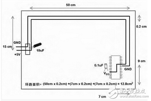
The above figure is improved by the fact that the power supply and ground are close to the trace, which reduces the loop area and reduces electromagnetic interference (679/12.8, about 54 times). Therefore, the power supply and ground should be as close as possible to the trace! The signal lines should be avoided and the lines should be avoided as much as possible to reduce the mutual inductance between the signals.
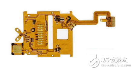
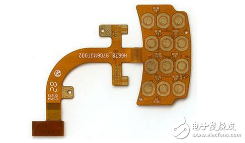
What is the difference between single-layer FPC/double-sided FPC/multi-layer FPC?PCBs are used in electronic products, and the market trend of PCBs is almost the vane of the electronics industry. With the development of high-end, miniaturized electronic products such as mobile phones, notebook computers and PDAs, the demand for flexible PCBs (FPC) is increasing, and PCB manufacturers are accelerating the development of thinner, lighter and denser FPCs. Edited to introduce you to the types of FPC.
The layer has a chemically etched conductive pattern, and the conductive pattern layer on the surface of the flexible insulating substrate is a rolled copper foil. The insulating substrate may be polyimide, polyethylene terephthalate, aramid fiber ester and polyvinyl chloride. Single-layer FPCs can be divided into the following four subcategories:
1. No overlay single-sided connection
The wire pattern is on the insulating substrate, and the wire surface has no cover layer, and the interconnection is realized by soldering, welding or pressure welding, which is commonly used in early telephones.
2. Covered single-sided connection
Compared with the previous class, it only has a layer of cover on the surface of the wire. The pad needs to be exposed when covering, and it can be easily covered in the end area. It is the most widely used and widely used one-sided flexible PCB, and is used in automobile instruments and electronic instruments.
3. No overlay double-sided connection
The land interface can be connected to the front and back of the wire, and a via hole is formed in the insulating substrate at the pad. The via hole can be punched, etched or otherwise mechanically prepared at a desired position of the insulating substrate. to make.
4. Covered double-sided connection
In the different types of the former, the surface has a covering layer, and the covering layer has a passage hole, which allows both sides to be terminated, and still maintains the covering layer, and is made of two layers of insulating material and a layer of metal conductor.
The double-sided FPC has a conductive pattern formed by etching on both sides of the insulating base film, which increases the wiring density per unit area. The metallized holes connect the patterns on both sides of the insulating material to form a conductive path to meet the design and use functions of the flexibility. The cover film protects the single and double-sided wires and indicates where the components are placed. Metallized holes and overlays are optional, as required, and there are fewer FPC applications.
Third, multi-layer FPCThe multi-layer FPC laminates three or more layers of single-sided or double-sided flexible circuits together, and forms a metallized hole through a drill collar L and electroplating to form a conductive path between the different layers. This eliminates the need for complex welding processes. Multilayer circuits have tremendous functional differences in terms of higher reliability, better thermal conductivity, and more convenient assembly performance.
This has the advantage that the substrate film is lightweight and has excellent electrical properties such as a low dielectric constant. A multilayer flexible PCB board made of polyimide film is about 1/3 lighter than a rigid epoxy glass multi-layer PCB board, but it loses its single-sided, double-sided flexible PCB. Flexibility, most of these products are not required for flexibility. Multi-layer FPCs can be further divided into the following types:
1. Flexible insulating substrate finished product
This type is manufactured on a flexible insulating substrate and the finished product is specified to be flexible. This construction typically bonds the two ends of a plurality of single-sided or double-sided microstrip flexible PCBs together, but the central portions are bonded together to provide a high degree of flexibility. In order to have a high degree of flexibility, a thin, suitable coating, such as polyimide, may be used on the wire layer instead of a thicker laminate overlay.
2. Soft insulating substrate finished product
This type is manufactured on a soft insulating substrate, and the finished product is specified to be flexible. Such multilayer FPCs are laminated to a multilayer board using a soft insulating material such as a polyimide film, which loses its inherent flexibility after lamination.
Withstand high voltage up to 750V (IEC/EN standard)
UL 94V-2 or UL 94V-0 flame retardant housing
Anti-falling screws
Optional wire protection
1~12 poles, dividable as requested
Maximum wiring capacity of 4 mm2
Feed Through Terminal Block,T12 Series Terminal Blocks,Terminal Strips Connector,Cable Connectors Block
Jiangmen Krealux Electrical Appliances Co.,Ltd. , https://www.krealux-online.com