Review the history of interface technology development
With the rapid development of the Internet of Things (IoT), there will be massive amounts of data in the future. In the "big data" era, higher demands are placed on data processing. High-performance processors and clusters can complete real-time data processing. The large amount of data transferred between the processor and the peripheral or the processor also puts forward higher requirements on the interface technology. It's like a person who has a clever mind, but his nerves are "long", and he looks very "stupid". The current mainstream parallel interface technology is facing such a situation, and it has increasingly become a bottleneck.
Looking back at the history of interface technology development, in fact, data transmission was originally a low-speed serial interface (Serial Interface, referred to as serial port). In order to increase the total bandwidth of data, the first thing to think of was to increase the data transmission bit width and then further increase the rate. That is, the parallel interface (Parallel Interface, referred to as parallel port), and gradually replace the traditional low-speed serial port to become the mainstream. But with the development of parallel ports, its limitations have become more and more obvious. The high-speed serial (High Speed ​​Serial, HSS) interface technology has the advantages that it has a trend to replace the current parallel port. It is manifested as a significant increase in the total bandwidth of the interface. Its history is as shown in Figure 1. It has been upgraded from mountain trails to rural roads, and then to expressways (networks), which can provide higher traffic.

figure 1
At present, the main limitations encountered in the development of parallel ports are that, on the one hand, chip packaging is facing the problem of a tight IO quantity, on the other hand, the crosstalk and noise (SSN) problems faced by the parallel port data rate increase process, which make the data Synchronization becomes very difficult. This question can be understood as, just like a phalanx of a military parade, walking upright and valiantly, it takes a long time to train. If you are required to run in unison, you must also line up horizontally and vertically (data alignment and synchronization), which is really stumped.

figure 2
The alternate development and evolution of serial port and parallel port can really be described as "Hedong in 30 years and Hexi in 30 years". There is no right or wrong technology, and "the times make heroes".
The typical representative of the serial port is the Universal Serial Bus (USB) commonly used in consumer electronics and other fields; there are also many parallel ports, such as DDR DRAM memory interface, which is often referred to as DDR.
For the fast speed of serial and parallel ports, it depends on how to describe the problem.
In terms of line rate (linerate), for example, the maximum line rate of DDR3-1600 is 1600Mbps (that is, 1.6Gbps). Let's look at how much the current mainstream SerDes can achieve. The SerDes provided by Xilinx's 16nm Ultrascale+FPGA can reach a speed of 32Gbps. Recently, the dual-mode SerDes chip demonstrated by Credo Semiconductor has the performance of 112Gbps PAM4/56Gbps NRZ. Therefore, it is generally understood that the high-speed serial port is faster than the parallel port, mainly from the perspective of line rate.
Of course, from the perspective of total data bandwidth, for example, the maximum data bandwidth of 64bit DDR3-1600 also exceeds 100Gbps (64*1.6Gbps). Can also provide good overall bandwidth performance. In fact, SerDes can also be used in parallel with multiple channels, such as the x4, x8, and x16 modes of the PCIe protocol. Although there are also multi-channel alignment problems. But the total bandwidth presented will be relatively larger. The future development of high-speed serial port technology is still a combination of increasing the speed of a single channel and the parallel use of multiple channels. Therefore, the concept of serial and parallel ports may be further blurred. The overall result is to provide total data bandwidth for continuous improvement and upgrade.
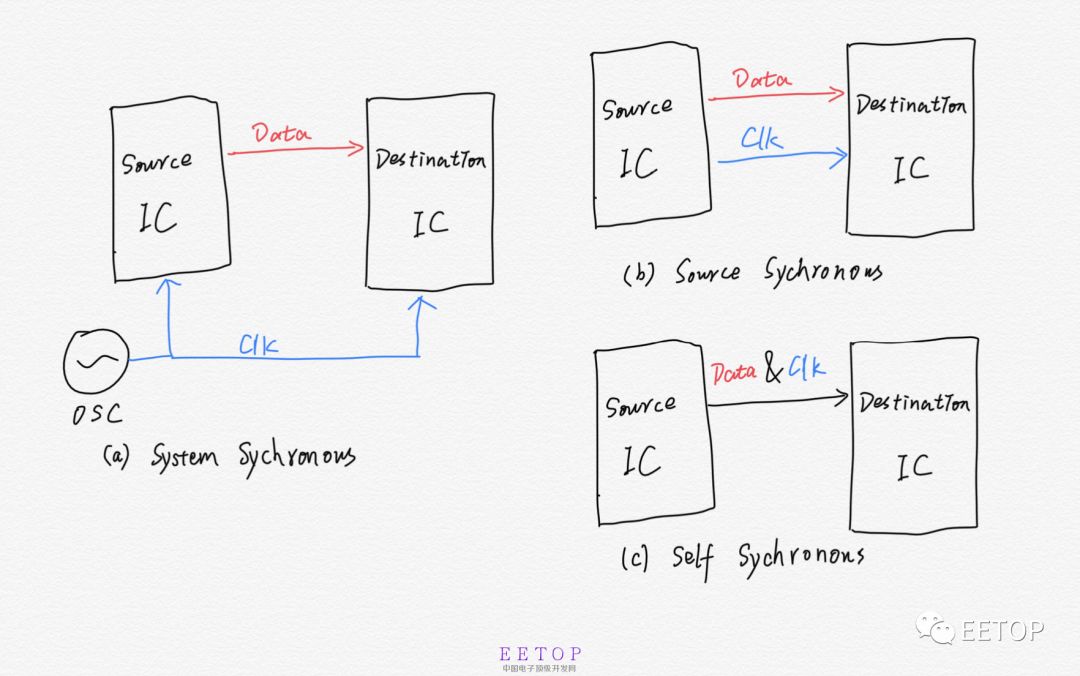
It is also necessary to understand the three basic timing models for communication between different chips through a synchronous interface. As shown in Figure 3 (a/b/c), they are system synchronization, source synchronization, and self-synchronization. The wiring delays at the board level and inside the chip are omitted in the figure. Initially, when the interface rate is low, the system synchronization method can meet the requirements. As the interface speed increases, the strict timing requirements will use the method of data and clock synchronization transmission, such as DDR data synchronization dqs clock line.

image 3
Self-synchronization is actually the method currently used in SerDes. The data transmitted by the interface contains clock information. The clock data recovery (CDR) circuit of the receiving end (Rx) completes the clock extraction and data reprocessing of the received data. sampling. Finally, the correct data is recovered.
For the SerDes technology used in High Speed ​​Serial Link, SerDes is the abbreviation of Serializer and Deserializer, and basically explains the principle of SerDes. It is to complete the parallel-to-serial and serial-to-parallel conversion. SerDes is a typical digital-analog hybrid system, which requires a lot of background knowledge. Digital circuits and analog circuits, signals and systems, communication principles, microwave and radio frequency circuits, electromagnetic fields, signal and power integrity, etc., have relatively high comprehensive requirements, which can be regarded as current Point-to-point (point-to-point) wired (wireline) communication technology hotspot.
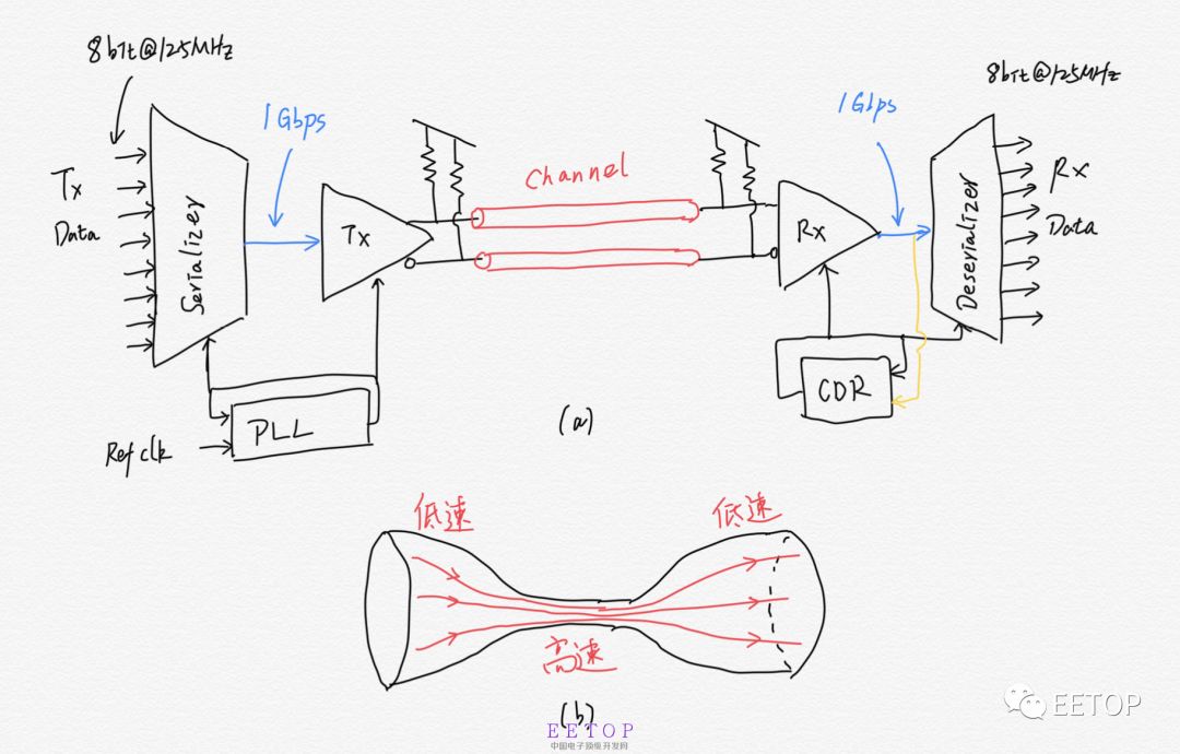
A simple schematic diagram of the SerDes interface is shown in Figure 4, and examples of data rates at different locations are given. In Figure (a), the 8-bit parallel data with a clock rate of 125MHz (a clock cycle of 8ns, a total of 8bit data), after serialization, is converted into 1Gbps 1bit serial data (one UI is 1ns, including 1bit data), and passes through the transmitter From the channel to the receiver, it is still 1Gbps after being processed by the receiver, and it is restored to 8bit parallel data with a clock rate of 125MHz after deserialization. This process can be visually understood as the low-speed Laval nozzle in Figure (b). The air flow goes from the cone with a gradually decreasing cross-section to a cone with a gradually increasing cross-section. "The flow velocity is small where the cross-section is large, and the flow velocity is high where the cross-section is small."

Figure 4
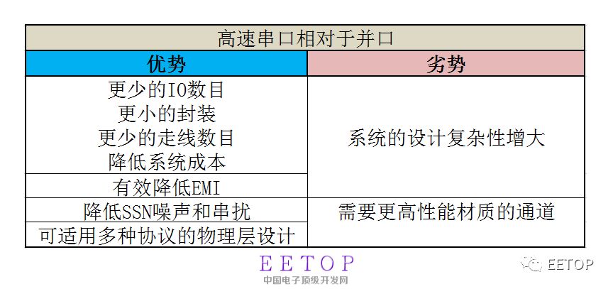
Figure 4(a) shows that SerDes is just a "simplex" form. It can be seen that the number of IOs can be reduced from 8 to 2 through serialization (most of the signal transmission adopts a differential form). It can effectively alleviate the problem of the shortage of chip IO numbers and reduce the complexity of PCB routing. From an economic point of view, smaller packages and fewer PCB traces, cables and connectors will reduce overall system costs. The main advantages and disadvantages of the high-speed serial port technology relative to the parallel port are summarized in the table in Figure 5.

Figure 5
From Figure 4(a), you can also get a glimpse of SerDes technology, which is mainly reflected in several aspects.
First, the generation of high-frequency and low-jitter clocks. For example, for a data rate of 10Gpbs, at least a 10GHz clock (Single Date Rate, SDR) or a 5GHz clock (Double Date Rate, DDR) needs to be generated internally. With the development of SerDes, the clock frequency of the internal PLL continues to increase. Ring PLL and LC tank PLL are both indispensable. The impact of clock jitter and various jitters on the bit error rate (BER) needs to be sufficient. analysis. High-performance clock is a technical focus of the entire SerDes system design.
Second, signal integrity considerations. In the content of the transmission line, we have a preliminary understanding of the irrational characteristics of the transmission line. With the increase of the data rate of the signal and the increase of the channel length, the data sent by the transmitter (Tx) will be attenuated and inter-symbol interference (ISI) after passing through the channel. Existence makes the signal at the receiver (Rx) end disappear. In order to recover the data correctly, it is necessary to equalize the attenuation of the channel and the inter-symbol interference of the data through an equalizer. For example, common methods such as Tx feedforward equalization (FFE), continuous time linear equalization (CTLE) and decision feedforward equalization (DFE) at the Rx end.
Third, the adaptive algorithm. Equalization at the Rx end usually needs to meet the characteristics of channels of different materials and lengths, and compensate for the attenuation of different frequency components of the signal. CTLE and DFE usually use self-adaptive algorithm (Self-Adaptive Algorithm) to dynamically adjust in real time to cope with changes in channel characteristics. If you don't understand the algorithm implementation, you can't understand the essence of DFE accurately.
There are many textbooks on adaptive algorithms, such as "The Principle of Adaptive Filter" by Simon Haykin. Hey, I regret that I didn't study mathematics well, but I am still gnawing slowly. It can only be said that it is difficult to understand.

Figure 6
Fourth, the CDR loop. Another difficulty on the Rx side is the CDR loop. There are different ways to implement CDR. The CDR loop usually contains a large number of digital implementations, and accurate understanding is also very important. The understanding of this part is still learning, and I will share it with you when I have the opportunity.
Fifth, timing constraints are restricted. When the data rate increases, higher requirements are put forward for the timing design of the decision feedback loop of the DFE. For example, for a 50Gbps SerDes, the time for a UI is 20ps, which is almost equivalent to the delay of a logic gate. This requires the logic design of the DFE's feedback loop to be as simple as possible. The clock rate alone will encounter difficulties, and the use of signal methods such as PAM-4 or PAM-8 will appear very promising.
SerDes is a complex digital-analog hybrid system that also contains a large amount of digital realization content. Codec implementation such as 8B/10B, PRBS generation and inspection, loopback test, adaptive algorithm implementation, system status control digital implementation, etc.
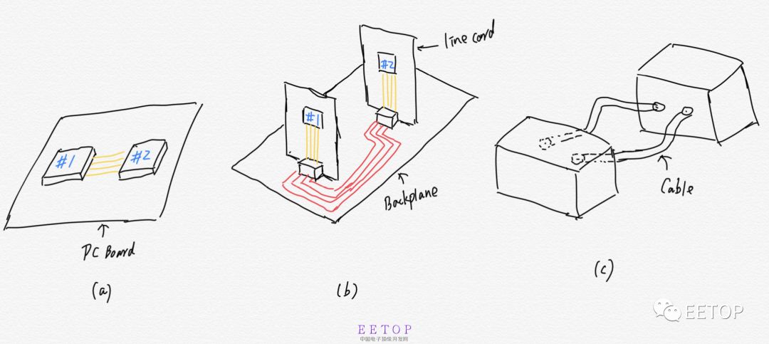
The current SerDes applications mainly include Chip-to-Chip, Board-to-Board, Box-to-Box, etc., as shown in the schematic diagram of Figure 7 (a/b/c). And it has applications in large-scale data centers, communication backbone networks, consumer electronics and other scenarios.

Figure 7
Different application occasions have also given birth to different protocol standards. Such as PCI Express, Serial ATA, Ethernet, Serial RapidIO and Aurora. Different protocol standards have different rates and are constantly evolving. Figure 8 lists the data rates of several protocols. At present, the line rate of a single channel is mainly concentrated above Gbps.

Figure 8
From a protocol perspective, different protocols usually have different layered definitions. Most of the SerDes hardware implementations we are concerned about are concentrated on the physical layer. Of course, a higher level understanding of the protocol can help a better understanding of the underlying hardware implementation.
The full name of the abbreviated term in the attached text:
NRZ Non-Return to Zero
PAM-4 Pluse Amplitude Modulation-4 level
SerDes Serializer/Deseiralizer
Gbps Gigabit per second
CTLE Continuous Time Linear Equalization
DFE Desicion Feedback Equalization
FFE Feed Forward Equalization
ISI Inter-Symbol Interference
PRBS Pseudo-Random Binary Sequence
Goldshell Miner:Goldshell Mini-DOGE Pro,Goldshell LT Lite,Goldshell X5,Goldshell LT5,Goldshell LT5 Pro,Goldshell LT6,Goldshell Mini-DOGE
Goldshell Miner is an industry-leading technology company. The company was founded in 2017, we are focusing on high-performance miners and application fields. In the past few years, Goldshell Miner has successfully completed the R&D, mass production, and sales of multiple miners in LTC, CKB, HNS, Sia and other cryptocurrencies. The headquartered is based in Shanghai, Goldshell Miner has offices in Hangzhou, Hong Kong, Singapore,etc. The current R&D personnel account for more than 70% of the company. The core team has more than 10 years of experience in the integrated circuit field. Aiming to become an excellent blockchain computing power provider, and promoting the development of the industry, Goldshell has established an efficient operation system from algorithm research, batch production and delivery, which based on a strong core team and excellent system capabilities. Goldshell continuously improved the computing performance and competitiveness of products, to provide high-performance and high-reliable computing infrastructure and services for the development of digital economy. Especially our household miner-BOX series, allow more customers to join in the market since our product are small, quiet, affordable, and friendly to beginners so that everyone could start mining at home.
goldshell mining machine,goldshell ltc miner,goldshel lt5,goldshell mini doge pro,goldshell lt6
Shenzhen YLHM Technology Co., Ltd. , https://www.asicminer-ylhm.com
