Semiconductor Industry Sets Up Convergence The United States Blocks Chinese Outbound M&A
[Semiconductor Industry Sets Up Convergence in the United States to Block China's Outbound M&A] There is a significant gap in the IC industry in China compared to the rest of the world. What is the road to catch up?
How does China plan to overtake China's core?
In 2014, the State Council issued the "Outline for Promoting the Development of the National IC Industry" and hoped to accelerate the mass production of the 16/14nm manufacturing process. At the same time, it is hoped that by 2030, the major links in the IC industry chain will reach the international advanced level, and a group of companies will enter the first international team and achieve leapfrog development.
Subsequently, China also established a national integrated circuit industry investment fund ("big fund") to invest in domestic semiconductor companies. The first phase raised funds of 138.7 billion yuan. By 2017, local governments will jointly announce the establishment of a semiconductor fund worth 500 billion yuan; Drive social investment by 700 billion yuan.
In 2015 China Made 2025, it was proposed that the self-sufficiency rate of Chinese chips should be raised from less than 20% in 2015 to 40% in 2020 and 70% by 2025.
However, industry insiders who do not wish to be named pointed out that, on the one hand, China started late in the modernization of integrated circuits, and the replacement rate of integrated circuits is very fast; on the other hand, the United States and other countries implement strict export to China in related industries. Regulations prevent multinational equipment suppliers from shipping the latest equipment to China. This makes China's integrated circuit industry development limited by technology.
The person said that technology is not easy to transfer, and it is not only composed of blueprints and formulas that can be delivered on demand. More importantly, the knowledge of the numerous problems encountered in the design and production process and their solutions are obtained through experience. This knowledge can only be transferred through long working assignments between the assignor and the assignee. At the same time, the success of the technology is difficult to obtain. It depends on the willingness and motivation of the transferor, as well as the capacity gap between the transferor and the transferee.
In countries such as Japan and South Korea, they have not opened up their economies to foreign capital, nor have they provided markets for technology. In terms of technical capacity building, these countries have limited cooperation with foreign companies and can only emphasize self-study through well-designed national projects.
The above-mentioned sources stated that through this method, Japan and South Korea can bring the technological level of their cars, semiconductors and other industries to the international frontier for several decades. “But in the case of a large distance, this will cost A lot of time, until the R&D comes out, technical progress may throw you off again."
Guo Gaohang believes that on the equipment side, the current 8-inch market for the sale of used second-hand production lines is in short supply. It is an opportunity for domestic equipment to solve domestic equipment verification problems.
Firstly, increase the domestic penetration rate of the packaging and test equipment market. Traditional packaging and high-end packaging equipment will be promoted synchronously. Supporting local equipment leaders will give priority to the layout of high-end processes in some key wafer manufacturing equipment fields, spurring China's mainland pilot line and China. Mainland manufacturers have increased their efforts in the verification of domestically-manufactured equipment. In addition, they have promoted the further consolidation and upgrading of equipment companies in mainland China, prompting the rapid improvement of the overall technological level of the domestic semiconductor equipment industry.
On the material side, Guo Gaohang believes that key materials such as silicon wafers, photoresists, high-purity chemicals, special gas and other materials need to continue to increase R&D investment and accelerate the mass production process.
Semiconductor Industry Sets Up Convergence The United States Blocks Chinese Outbound M&A
While increasing investment in the semiconductor industry in China, the tide of semiconductor industry integration is also sweeping the world. From 2015 to 2017, Intel, Qualcomm, Avago, and Western Digital have all actively launched billions of dollars of purchases, and Softbank also spent about US$32 billion to acquire ARM, the global IP leader.
Chinese capital and enterprises are also actively involved, but they are not high in terms of M&A and M&A success rates. Shawn Cooley, a special adviser to Freshfields Bruckhaus Deringer, told 21st Century Business Herald that two years ago or earlier, the U.S. Foreign Investment Committee’s concerns about the foreign acquisition of U.S. semiconductor companies were relatively limited.
“The situation changed in late 2016,†Cooley pointed out. At that time, overseas investment by Chinese-funded enterprises reached a record culmination, which led President Obama to block China’s acquisition of Aisikang. Since then, the U.S. Foreign Investment Commission has increasingly publicly stated that it needs to protect the U.S. strength in the semiconductor field and that it has become more aggressive in its review of foreign acquisitions, especially for Chinese-funded enterprises.
After President Trump became in power, the U.S. Foreign Investment Commission tended to avoid risks and its subsidiaries were reluctant to assume any potential risks. Cooley believes that this change is of great importance because the U.S. Foreign Investment Commission originally intended to manage risk rather than eliminate all risks.
In January 2018, the Chinese semiconductor company, North China Creation, acquired Akrion Systems LLC, a US semiconductor equipment manufacturer, for US$15 million. The U.S. Foreign Investment Commission approved the acquisition of AkrionSystems. Cooley believes that this case also shows that the focus of the U.S. Foreign Investment Committee is still to protect sensitive semiconductor technology, rather than related downstream industries.
Guo Gaohang believes that China’s national will in the development of integrated circuit industry is firm, while the entire industry chain is rapidly improving, and various industrial chain links are advancing at a high speed. In the future, once China has achieved independent control in the field of integrated circuit industries, the United States is the largest in the world. The status of exporting countries of integrated circuit products will be greatly threatened.
Maintaining the absolute superiority of China's IC industry for a long time is the focus of work that the United States considers. Guo Gaohang believes that directly influencing or blocking China's foreign mergers and acquisitions is one of the strategies to limit the growth of China's IC industry.
The aforementioned private equity person also stated that in the semiconductor industry, for example, the design side, there are very few overseas M&A targets, and there are several companies such as ARM, Intel and Qualcomm. The investment amount of some projects is hit by hundreds of billions, and the profit after M&A is not guaranteed. This will require a long period of time, and the investors' vision needs to be long-term.
Cooley pointed out that the U.S.’s current concerns about foreign investment in the telecommunications industry have risen sharply. “This is not just for China, but I personally think that this concern has not reached a peak.â€
Large Infrared Touch Frame (Splicing)
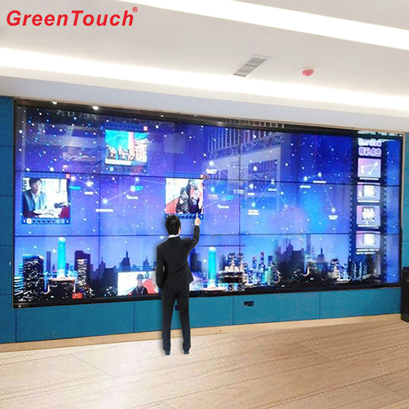
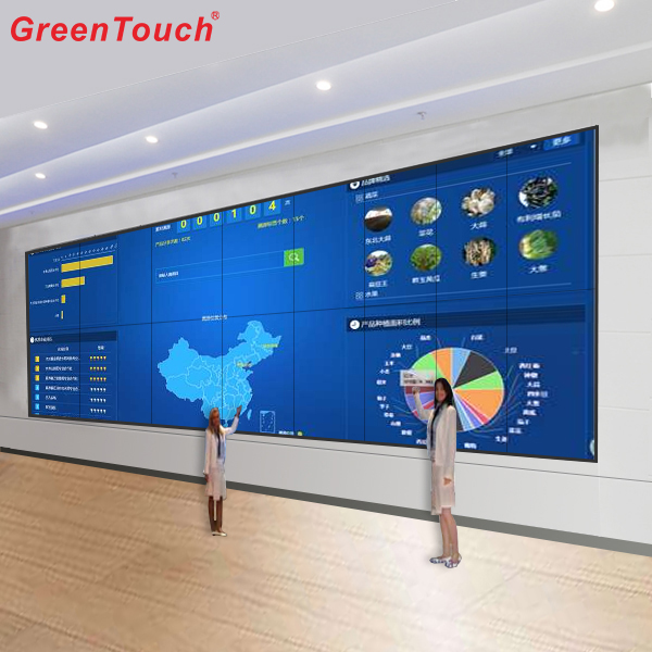
The splicing touch frame is an important part of the touch splicing screen system. Compared with other media propaganda carriers, the touch splicing screen reflects the extensiveness, intuitiveness, and fun of human-computer interaction and presentation, and has a strong visual impact. It has made a big step forward in the development of the touch industry. It is also a promoter of super-sized display integrated touch. The large-sized spliced touch TV display wall has involved schools, shopping malls, banks, digital exhibition halls, corporate exhibition halls, and government Institutions and military command can be equipped with digital content, interactive games, animation, 3D, VR, interactive audio and video, etc. It is an indispensable and effective application device for today's interactive large-screen demonstrations.
pictures show
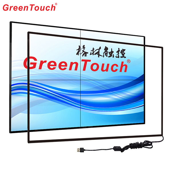
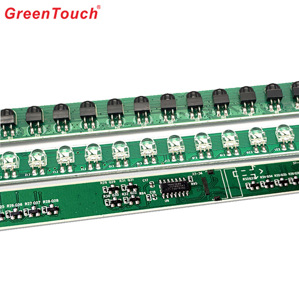
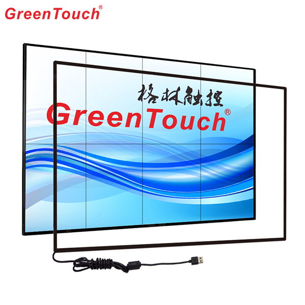
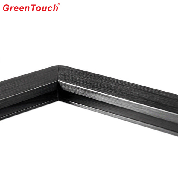
Large Infrared Touch Frame,Large Splicing Infrared Touch Frame,Ir Multi Touch Frame,Led Touch Screen TV Wall,Large-size Infrared Touch Screen,LCD Touch Screen TV Wall
ShenZhen GreenTouch Technology Co.,Ltd , https://www.bbstouch.com
