Switching power supply secondary synchronous rectification unlock
1. When is the SR open and when is it turned off?
(In a word, first attach the BCD chip circuit diagram)
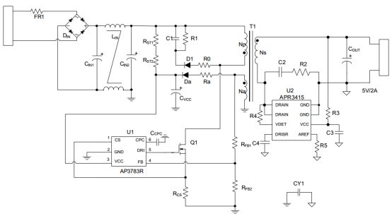
figure 1
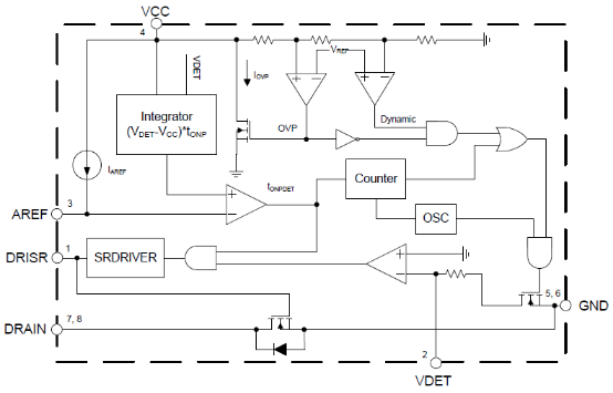
figure 2
The APR3415 on the secondary side in Figure 1 is the protagonist of this chapter. Figure 2 is the internal block diagram. It can be seen that the rectification MOS has been integrated into the chip (shown by the red circle).
Then when should he be opened? The criterion is actually thought out: he should be turned off when the primary side is turned on, and he can be turned on when the secondary side is turned on. But he is not the locust in the belly of the original control chip. How do you know when it should be turned on? We know that when the primary side MOS Q1 is turned on, it is judged that the secondary side is not the same name end according to the same name of the transformer (the same name of the black circle of the transformer T1, and the non-identical end of the black point), that is, the APR3415 The end of the DRAIN PIN connection is positive, then he must be turned off at this moment.
When the primary MOS is turned from off to off, the end of the same name is reversed, and the end of the secondary side connected to the DRAIN PIN is negative, then the rectification MOS can be turned on at this time, as shown in FIG.
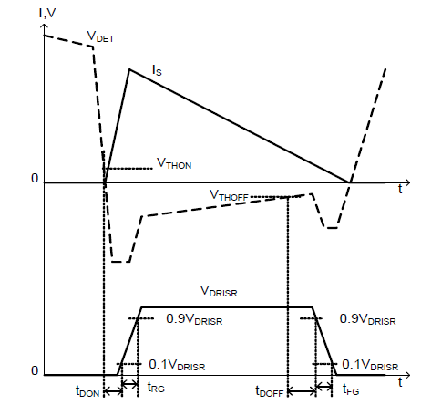
image 3
The VDET PIN detects the voltage of the DRAIN PIN through the resistor, so the potential is the same as DRAIN. When the voltage of DRAIN PIN changes from positive to negative, it will naturally drop and fall below a threshold voltage point VTHON (0V~1V). When VDET PIN detects below this threshold voltage, it passes an internal fixed delay TDON. After (70 ns), the MOS transistor is driven, and the MOS starts to conduct. Before the MOS is not turned on, the body diode continues to flow, so the DRAIN PIN will have a relatively large negative pressure (inside the red circle). When the MOS is turned on, the current is diverted by the body diode through the MOS.
However, the banquet in the world, the secondary side conduction current flowing through the MOS will decrease linearly with the secondary side voltage degaussing the secondary side inductance. If the freewheeling current has dropped to 0, you Still not shutting down MOS, when is it turned off? Have you kept off the New Year? If the freewheeling current is not turned off at the end, the secondary side capacitor will reversely charge the secondary side inductor, and the current will flow backward; if the primary side is turned on, the secondary side MOS is still turned on, which is called common , then it will be even worse. So it is important to grasp the timing of the secondary side shutdown. . .
The sweetest and most beautiful case is that the MOS turn-off helps the efficiency when the freewheeling current drops to zero. However, Li Jiacheng’s grandfather said that he never made the last piece of copper, so we should be close to 0 when the current is approaching zero. Turned off MOS, sacrificed point efficiency in exchange for reliability, huh, huh. Then the shutdown threshold is called VTHOFF (-20mv, -5mv). Once the VDET PIN detection crosses this threshold, the MOS is turned off after a fixed delay of TDOFF (100ns). After turning off, it is necessary to continue to flow through the body diode, so there will be a relatively large negative pressure (in the purple circle). If the primary side voltage sampling happens to be taken at this time, then the output voltage will not be good. Stable, about the PSR primary chip voltage sampling is also a learning, there will be a chance to talk later.
Summary: Determine the conduction is based on VDET PIN detection voltage is lower than VTHON (0V ~ 1V), determine that the shutdown is based on VDET PIN detection voltage is greater than VTHOFF (-20mv, -5mv)
Two: How does the rectifier chip distinguish the primary conduction waveform and the RING
Speaking of this, it seems to be finished, in fact, there is no (help me with a face expression). Actually, it is more complicated than ideal. First, when the rectification MOS is turned on, there will be RING Chinese name called ringing in DRAIN PIN. If the size of RING is higher than VTHOFF, it will cause MOS to be turned off in advance, which is often said. It's over at the beginning~ The youth is aging before it blooms~ So here is a minimum ON time Minimum ON Time inside the chip, the purpose is to shield this short time RING, forcing the conduction for a short time until the RING is eliminated. .
Also, if only the VDET PIN voltage is only turned on below VTHON, what should the RING in the middle dead time before the degeneration of the secondary side is completed before the primary side is turned on? Wait, how is RING? We know that after the degaussing, the primary inductance LP and the output capacitance of the primary MOS and other stray capacitances will oscillate happily for a while. This oscillation is a damped oscillation and will disappear after a while. Coupling to the VDET PIN through the transformer before the RING disappears will also cause the detection voltage to be lower than VTHON, but at this point the synchronous rectification MOS is not conductive, so we should add a condition to the secondary side synchronous rectification conduction. , see Figure 4 first.
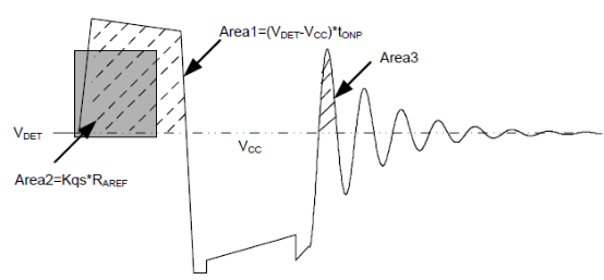
Figure 4
Figure 4 shows the voltage waveform of the VDET PIN over a whole period, including the primary side conduction, the secondary degaussing, and the three stages of the dead time before the degaussing is completed until the primary side is turned on:
Area1 is the area of ​​the box in the point slip line, which corresponds to the moment when the primary side is turned on. Its height = Vdet-Vcc (Vdet is the voltage of the vdet pin, Vcc is the voltage of the Vcc pin, because Vcc and the output voltage Vo is connected by a 20ohm resistor, and the voltage drop across the resistor is small, so the VCC voltage can be regarded as the output voltage Vo), and the width of Area1 is the on-time of the primary side Tonp, Area1=(Vdet-Vcc)* Tonp (voltage X time = volt-second product)
Area3 is the area of ​​the RING in the dead time (the voltage X duration of RING), and it can be found that Area1 is significantly larger than Aera3. Therefore, if the synchronous rectification chip has a function of the size of the area at this moment, the Area1 and the Area3 can be distinguished.
The following is a brief explanation of the circuit implementation of the logic function of the area: To distinguish, first we need a comparator Tonpdet to distinguish (see Figure 2 in the green circle), and secondly the area here is = voltage X time, can put the voltage and Time. These two parameters are combined into a device for electrical signal. We should naturally think of the integrator. Because the characteristic of the integrator is to add a voltage signal to the input, the output will also generate a voltage signal, and As the time continues to accumulate, the output voltage is constantly increasing, and the magnitude of the voltage at the input determines the magnitude of the rising slope. The integrator is shown in Figure 5. When a constant voltage ui is applied to the input terminal, a constant current i=Ui/R1 (the virtual short push of the op amp) is formed. The constant i only passes through the capacitor C1 (the amp of the op amp) Combined with KCL, it will form a constantly increasing voltage waveform with a constant slope as time: U=i*t/C (where t=Tonp) (waveform of the relationship between input voltage Ui and output voltage vo) As shown in Fig. 6, it can be found that the higher the ui, the more the slope will be shaken, the faster the rate of rise, and the longer the torp time is, the longer the rise time will be. The two will eventually determine the highest voltage rise vo)
Since the voltage ui and the duration tonn of the VDET PIN when the primary side is turned on are both greater than RING, there is a significant difference between the high and low output voltages Vo generated by the integral line. The difference is synchronous rectification. Judgment provides sufficient space (the final area size comparison is converted to the Vo voltage size comparison, and the integral circuit completes the electrical signal transition)
Connect Vo to the positive side of the comparator
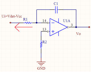
Figure 5
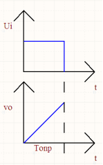
Figure 6
The negative terminal of the comparator is connected to the current source Iaref, the current is connected to the AREF PIN, and the AREF PIN is connected to a resistor R to generate the voltage Varare2=Iaref*R. Cough, knock on the blackboard! This voltage is the threshold voltage Area2 we set, which is used to distinguish between Area1 (the output of the integrator Vo1) and Area3 (the output of the integrator Vo3).
When the output of the integrator Vo is greater than the negative terminal voltage of the comparator, the output of the comparator is high to the AND gate of the drive, making it possible to turn on the MOS driver. Otherwise, the output is low, then the MOS driver is masked.
The following details are how to set the threshold voltage level Area2=Kqs*Raref (Kqs is Iaref, which is the chip internal parameter, the range is 0.325~0.515). We have to consider the case of the most worst, that is, the minimum on-time and the lowest voltage of the primary side are still satisfied when the Area1 is the smallest: Area1>Area2>Area3, and Area3 is determined after the system is determined. Area2 is the part we play, and it can satisfy the above relationship according to the actual debugging of the waveform. Usually, the Raref size is 37K. After adjusting the synchronous rectifier chip, you can separate the waveform of the original side and the waveform of the Ring!
Because the Arearf pin is very close to the Vdet pin, it will be disturbed by the Vdet pin, causing fluctuations in the threshold voltage. It is recommended to add a filter capacitor, Caref, but the larger the capacitance, the better, because the current source also charges the capacitor. The threshold voltage rises relatively slowly. After the output voltage is established, the threshold voltage may not be established yet, and the original function will be lost, causing the original secondary side to be common or even burned. I have encountered such a bomber situation, most of which occurred at the moment of the start of the bombing machine, the reason is also a lot of brains to find. . . So the capacitor is good, but don't be greedy, oh, no, don't be too big. The recommended value is 2.2nF. The value of the component is a learning. It is not the bigger the better, the smaller the better, the appropriate value. Zhang Fei often talks about the various components in his video. Value problem.
Three: how to monitor the secondary side voltage
In many markets, PSR chargers are basically PFM. When entering light load or no load, the output frequency will be very low. For example, the full load is 60KHZ, then 100HZ at no load. The sampling mechanism of PSR for output voltage is as follows: The pulse is output and waiting for the secondary side to demagnetize until the secondary output voltage is high or low, and then regulated. Therefore, the following phenomenon will occur: when the airborne steady state is calm, the working frequency is very low, and 100HZ will only make a pulse, and suddenly a lightning strikes through the air! Oh, no, it is suddenly switching the output current from no-load to large load or even full load. Then the output voltage will have a big drop. It can only be detected after the next cycle may be 100HZ. The reaction can't be tolerated. (At this time, the SSR is crushed. No way, who is called SSR born with a combination of TL431+ optocouplers? What is the wind on the secondary side can immediately notify the original side)
In response to this situation, we can use the rectifier chip VCC pin to monitor the output voltage. For example, when the output voltage is lower than a certain threshold, such as 5.25V, we will tell the original chip to the situation and let the original side quickly pulse. ! But how do you notify the original side? The secondary side chip has no mobile phone, no optocoupler, and a transformer separated from the original chip. . . Wait, transformers, transformers are not the best way to pass signal coupling signals? Yes, we can tell the original chip through the transformer! The transformer is usually coupled with a voltage signal. If we close the secondary side MOS, the output voltage can be clamped on the secondary side inductor, and then there is no voltage on the primary winding. Then the FB pin of the primary chip can sense the voltage through the auxiliary coil winding and can immediately pulse.
Well, the idea is good, just a little bit of the secondary side MOS is turned on a bit, the energy on the secondary side is too large, the energy absorbed from the output capacitor is too much, and the charger will test the reverse leakage at the output. The current test, so the test should not pass. . . What should I do? Nothing, not to say that the energy is too big, then the energy is small, so in the chip we have integrated a RDSON larger MOS (in the yellow circle of Figure 2), and the MOS is also connected in series with a resistor and then connected to VDET PIN, and then connect the resistor to DRAIN PIN by VDET PIN. By turning on this RDSON big MOS, we can send out the signal we want but not too big. The specific signal propagation waveform is shown in Figure 7:
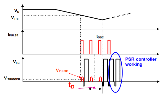
Figure 7
When the output voltage Vo is lower than the threshold value Vtrigger, the secondary side small MOS is turned on and off periodically by tosc (about 30 us) to cause a single current pulse Ipulse, which is coupled to the primary FB PIN through the transformer. Afterwards, a number of small-scale Vpulse are generated. As long as one Vpulse is higher than the threshold voltage determined by the primary side, such as 83 mv, the primary side immediately pulses to supplement the secondary side energy while monitoring the secondary side voltage. So very good, but still the old saying, after the secondary side degaussing, there will be RING, the original FB PIN is how to distinguish this is the RING or the secondary side CALL pulse? Hey, is this question familiar? Please think about it here, I will have a chance to write this article later.
The above-mentioned mechanism of the secondary side of the secondary side will lead to another by-product: when entering a very light load or no load, we can completely hand over control to the secondary side, let the original chip go to sleep! (turn off the modules in the original chip) Only leave the FB detection module awake (the advantage is that the power consumption of the chip can be reduced). Once Vpulse is detected, wake up and pass the primary MOS with only the smallest Ilimt. Gentlely shoot a pulse to pass energy to the secondary, then the original chip goes to sleep! In this way, even if there is no dummy load on the secondary side voltage, the output will not go up at no load, which reduces the standby power consumption and reduces the dependence on the dummy load. At this time, the output voltage of the no-load is equal to the Vtrigger voltage.
However, the primary chip always consumes the charge on the VCC capacitor. If the secondary side output voltage is stable at no load and has not dropped to the Vtrigger value, the voltage on the primary VCC capacitor will continue to drop until the primary side is triggered. UVLO (undervoltage restart), then the secondary side will pulse again to the original side, it will not be ignored, because the original side itself has to go through a long VCC voltage restart process. So how to avoid the original VCC restart? We have to forcefully increase the turn-on cycle time Tdis (30ms), which means that every 30ms above Vtrigger, whether or not you drop Vo to Vtrigger, I have to force a pulse to wake up the primary side. , for nothing else, just to power the VCC capacitor. However, the output voltage may be larger than Vtrigger when the load is no-load. If you want the output voltage to drop, you can reduce the Ilimt at no load. what? Will not fall? Increasing the resistance of the current sense resistor Rcs is good, or reducing the transformer's inductance, you can't add a dummy load properly.
Now, let's talk about the small load or even no load of full load switching. Switching from full load to small load will inevitably cause an Overshoot at the output. This is essentially an extra energy. If there is a path to bleed this excess energy. It will be fine. So we integrated a MOS tube inside the chip. The MOS tube in the black circle of Figure 2 is. When the output voltage is higher than a certain threshold Vdis such as 5.35V, the VCC pin will pull an Idis from the output capacitor. 3mA current, if 3mA still can't pull overshoot the rising momentum, when the output voltage is higher than Vovp such as 5.8V, then the code is chaotic! VCC pin directly pulls Iovp about 100mA to strongly suppress the overshoot trend, but 100mA current through 20Ohm resistor to VCC pin, the voltage drop is easy to have 2V, and lower than the Vovp threshold, which will lead to shutdown Vent MOS. . . Some people will say that the 20ohm resistor is removed, then you go, ESD has been played, if there is no way to do it? Intimate chips have been thought of, OVP once triggered a tovp_last about 2ms of discharge time, tovp_last after stopping the bleed and then detect the VCC pin voltage, if it is still higher than Vovp then continue tovp_last time and then discharge until the voltage drops below Vovp . Therefore, Vovp function is a good helper to suppress overshoot, and Vtrigger is a good tool to suppress undershoot. These two functions perform their own functions, which solves the problem of PSR's inherent dynamic response.
By the way, if the overshoot is higher than Vovp, the secondary chip will stop calling the ring to the original chip. Why stop the pulse? The secondary side voltage is already very high, and then let the primary side chip pulse the energy to the secondary side is not added? At this time, if you encounter the problem that the output voltage drops linearly below the spec after the full load is cut, it is not too pleasant. It is because the secondary side is in full swing, but the primary vcc capacitor is cold and clear, and the secondary The side still does not hit the pulse to wake up the original side, so in the long run, the original side chip directly strikes into the uvlo. . . .
Attached to Figure 8 is a more intuitive understanding of the whole process I mentioned above (Von is the working voltage of the chip is about 3V):
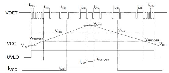
Figure 8
L Series Lead Acid Battery,Custom Valve Regulated Battery,12V 38Ah Battery,12V 65Ah Lead Acid Battery
Wolong Electric Group Zhejiang Dengta Power Source Co.,Ltd , https://www.wldtbattery.com
