Technical Contrast Analysis of Surface-Conduction Electron Emission Display (SED) and Field Emission Display (FED)
The field emission display (FED) light emission principle is that a high voltage is introduced into the vacuum belt between the transmitting and receiving electrodes to generate an electric field, so that the electric field stimulates the electrons to hit the phosphor powder under the receiving electrode, thereby generating a luminescence effect. This kind of luminescence principle is similar to a cathode ray tube (CRT) in which the electrons collide with the phosphor powder in a vacuum. The difference lies in that the CRT emits an electron beam from a single electron gun and is controlled by a Deflation Yoke. The electron beam emits the scanning direction, while the FED display has hundreds of thousands of active cold emitters, so the FED can achieve a space-saving effect on the structure than the CRT. Secondly, in the voltage part, the CRT needs about 15~30KV working voltage, while the FED cathode voltage is less than about 1KV.
FED Technology Principles and DevelopmentThe theory of field emission electrodes was first proposed by RHEowler and LW Nordheim in 1928. However, the actual development of field emission electrode elements using semiconductor process technology and the use of field emission electrons as display technology were proposed by CASpindt in 1968 and subsequently attracted. Follow-up investigators invest in research and development.
However, the application of field emission electrodes was not realized until 1991 after the French company LETI CHENG exhibited a display product made with field emission electrode technology at the 4th International Vacuum Microelectronics Conference. And attracted companies such as Candescent, Pixtech, Micron, Ricoh, Motorola, Samsung, Philips and other companies, but also make the FED join the ranks of many flat-panel display technology.
In field emission display applications, there is a vacuum zone between the transmitting and receiving electrodes. Therefore, a high voltage must be introduced into the transmitting and receiving electrodes to generate an electric field, so that the electric field stimulates the electrons to hit the phosphor powder under the receiving electrode, thereby generating a luminescence effect. This kind of luminescence principle is similar to a cathode ray tube (CRT) in which the electrons collide with the phosphor powder in a vacuum. The difference lies in that the CRT emits an electron beam from a single electron gun and is controlled by a Deflation Yoke. The electron beam emits the scanning direction, while the FED display has hundreds of thousands of active cold emitters, so the FED can achieve a space-saving effect on the structure than the CRT. Secondly, in the voltage part, the CRT needs about 15~30KV working voltage, while the FED cathode voltage is less than about 1KV.
Although the FED is regarded as a promising CRT technology, it was not able to compare with the cost of the CRT in the early stages of development. The main reason was that the field emission element was a problem. The earliest proposed Spindt-type micro-size arrays were the first to implement emission display technology, but its array characteristics limited the size of the display, mainly because its structure included a round hole in each array element. Containing a metal cone, lithography and evaporation techniques both limit the size of the process.
The solution is to use a technology that replaces the Spindt field emission device. After an article published by NEC on carbon nanotubes in 1991, the researchers found that graphite synthesized with a nanostructure or a carbon nanotube can be used as a field emission device. With better field emission efficiency, the carbon nanotube synthesis technology becomes a new direction for FED R&D.
At present, in the carbon nanotube field emission display field, Japan Ise Electronics and South Korea's Samsung invested relatively early, and SONY, Hitachi, Fuji Photo, Canon, Panasonic, Toshiba, Nikon and NEC and other manufacturers are also related to the proposed nanotechnology. The patent application, in which the carbon nanotubes as the main research and development projects.
In the large-scale field emission display panel, Japan Ise Electronics was the first devaluation. The company used chemical vapor deposition to successfully produce a 14.5-inch color nanometer carbon nanotube field emission display with a brightness of 10,000 cd/m2. In addition, Samsung in Korea Also announced is a single-color, 600cd/m2, 15-inch nano-carbon tube field emission display, and plans to develop a 32-inch nano-carbon tube field emission display for use in televisions, successfully achieving low-voltage drive results below 100 volts.
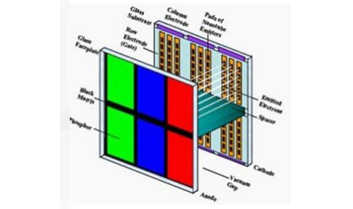
The same is used to bombard phosphors with charged particles, but the principle of SEDs generating electrons is very different from that of CRT displays. The electron gun of the CRT heats the metal cathode to make it surface active and generate active electrons. Then the anode is used to pull electrons out of the cathode, and the deflection yoke is used to allow the electron beam to scan at both the horizontal and vertical directions of the fluorescent screen. Generate a complete picture.
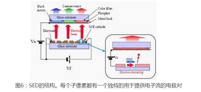
In contrast, SEDs not only do not have scanning devices, but also generate electrons in different ways. Each pixel on the SED screen has its own electron emission device (cathode). This electron emission device is actually a carbon nano-gap having a width of about 5 nm (nanometers). Since the gap width is extremely small, an electron flow can be generated by applying a voltage of about 10 V across the gap (this is the same principle as the charge and discharge of the memory cell in the flash memory chip, which is called "FN tunneling"). At this point, if a positive voltage is applied to the metal backplate (anode) and an electric field is formed between the electrodes and the cathode, the electron flow will escape from the gap under the influence of the electric field force, and run toward the anode, bombarding the phosphor, and emitting fluorescence.
Surface-conduction electron-emitter display (SED) technology advantagesThe special manufacturing process, together with the stable performance of the material, ensures the stability of the SED panel at room temperature.
More obvious advantages than liquid crystal and plasma
In the display and television markets, CRT technology has matured over the years, but due to volume and power consumption issues, the market performance has shown signs of fatigue, replaced by flat panel displays such as liquid crystal and plasma. However, these two flat panel display technologies are also not perfect display technologies, and they are still far from satisfactory in terms of display quality, power consumption, and price. With the emergence of SED, its excellent performance undoubtedly gave people the expectation of this new display product. Professor Nihonori Hiroshi, director of the Advanced Nanomechanics Laboratory at the Nano Vision Research Center at Shizuoka University in Japan, pointed out that SED will have a wide range of product applications in the era of luminescent displays and nanotechnology. He believes that SED will be an excellent choice for full-color high-definition television products. Compared with traditional flat panel display technology, SED has advantages in performance and cost.
From the aspect of display quality, SED uses the same phosphor as the ordinary TV picture tube, and its brightness can reach 400cd/m2. In terms of color saturation and sharpness, the SED is unmatched by LCD and plasma TV. Moreover, the SED emits light by electron bombardment of the phosphor and belongs to a self-light emitting device. There is no problem that the viewing angle of the liquid crystal display is insufficient and the response time is too long. SED light emission is completely controllable, there is no liquid crystal display backlight leakage or plasma display pre-discharge problems, the black brightness is only 0.04cd/m2, the contrast ratio in the dark is as high as 10000:1, black expression is extremely strong.
In terms of power consumption, the SED has a luminous efficiency of 5 lm/W and consumes about half the power of the same size plasma or LCD monitor.
In terms of cost, the structure of the SED is basically a planar structure, which is different from the three-dimensional structure of liquid crystals and plasmas. Therefore, advanced printing processes can be used for mass production, thereby increasing production efficiency and reducing costs. According to a report from TRI, the cost of a 40-inch SED panel can be controlled at $600, while the cost of the same-size LCD and plasma panels is around $700 (2008). However, taking into account the factors of the initial R&D expenditure, the current cost of the SED is still relatively high. However, by 2010, it will be equal to the LCD and plasma. As the scale of production increases, the cost advantage of SED will become more pronounced.
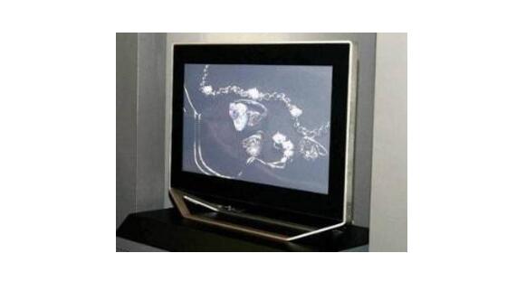
1, appearance
First of all, they are all flat-screen ultra-thin screen technologies that can meet the HDTV specifications for large-screen displays. An industry-proven SED flat-panel display with a diagonal size of 36 inches has (H) 1280X3X(V) 768 pixels. The display is only 7.3mm thick and consists of a 2.8mm thick cathode plate, a 2.8mm thick anode plate, and a 1.7mm thick vacuum barrier. This flat panel display weighs 7.8kg. Similar size FEDs are similar in weight and thickness, and the target markets for both FEG and SED are large-screen HDTVs.
2. Display Technology
Second, they are direct viewing or emissive display technologies. Each pixel or sub-pixel can itself generate light energy that is directly visible to the user and therefore can provide high contrast and efficiency, as well as other performance improvements. For SED and other FED technologies, the image-forming light is generated by a phosphor screen anode that is very similar to a cathode ray tube (CRT) anode screen with energy electrons. The phosphor layer used is also the same or similar to the CRT.
3, structure
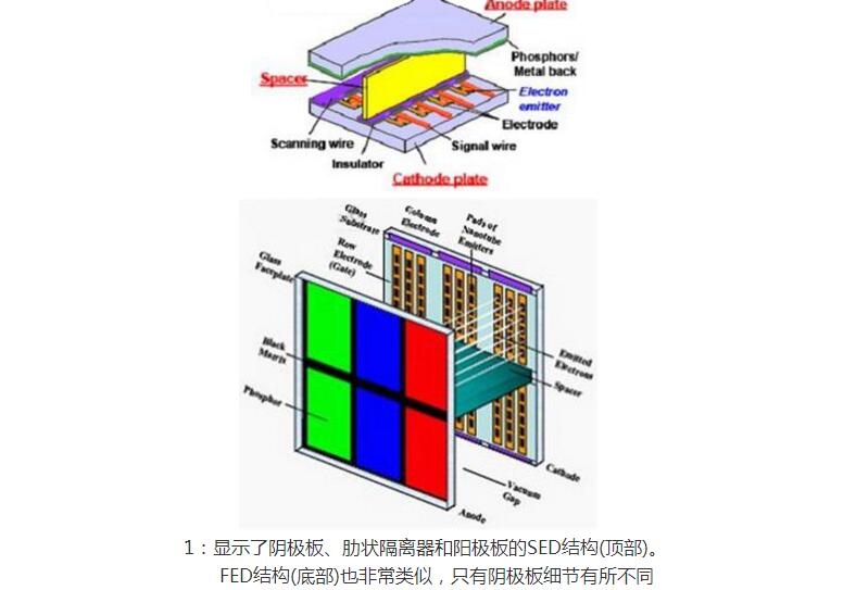
Third, because the electron acceleration requires vacuum to avoid corona or plasma discharge, the mechanical structure of the SED and other FEDs consists of a sealed glass envelope, which is vacuumed to form the vacuum required to accelerate the electron beam. Depending on the size of the display and the thickness of the glass wall, spacers are often needed to protect the glass wall from atmospheric pressure. The isolator must also be able to withstand high voltage gradients and be transparent to the user in normal operating conditions. The 36-inch SED requires 20 rib spacers to maintain a 1.7 mm thick vacuum gap. SED display schematic diagram shown in Figure 1. All FED technologies, including SEDs, require some form of suction technology in order to maintain the required vacuum inside the glass envelope after the display is evacuated and sealed.
4. Manufacturing
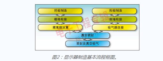
The last point is that the manufacturing and assembly processes are very similar, except for cathode plates, which will be discussed later. All FED technologies currently under development require the assembly of a front plate (anode) and a rear plate (cathode or electron source) as well as side walls, separators, and aspirator devices. The anode and cathode plates are fabricated separately, then assembled with other components, sealed with glass frit or other new materials, and finally vacuumed. Figure 2 shows the CNT-based FED assembly process, which is also suitable for other FED technologies including SEDs. Some technologies combine the sealing and vacuuming steps, while others eliminate the isolator or reduce the number of isolators. Some new materials under development are expected to replace the glass frit seals to reduce the sealing temperature and avoid the use of high-lead materials.
The anode fabrication process for SEDs and FEDs is very similar. Figure 3 shows the details of the anode structure of the SED panel: black matrix and color filters are used to increase contrast, metal back films are used to improve brightness and efficiency, and are also used as high voltage potential electrodes and are released from the phosphor layer during electron beam illumination. Out of charge.
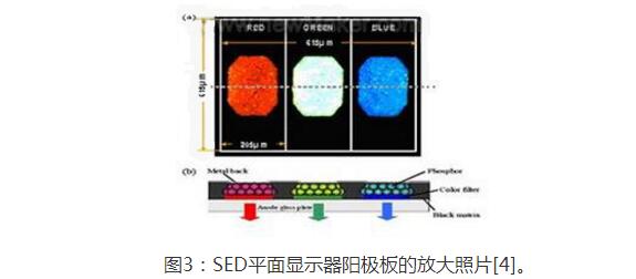
In addition, both SED and CNT-based FED displays use printed methods to fabricate anode and cathode plates (more on this later). From a personal perspective, therefore, SEDs and many other FED technologies have many of the same components, such as fluorescent layers, isolators, getters, and most assembly processes used on anodes and anodes. Let us look at the uniqueness of SED and other FED technologies.
The difference between SED and FEDThe significant differences between the SED and the FED can be clearly seen from the electron source board and the driver circuit. Before discussing the significance of differences, we must first understand the structure and working principle of each technology.
1. Standard FED transmitter structure
Some typical structures using carbon nanotube (CNT) emitters are shown in Fig. 4. Microtip transmitters have a similar structure. In both cases, the electron beam is formed by taking electrons from the emitter structure (CNTs or microtips), which is the result of the voltage difference between the anode, the gate, and the cathode resulting in a high electric field on the emitter. At some point, the anodic electric field causes electron emission, and the cathode-gate differential pressure controls the emission current intensity.
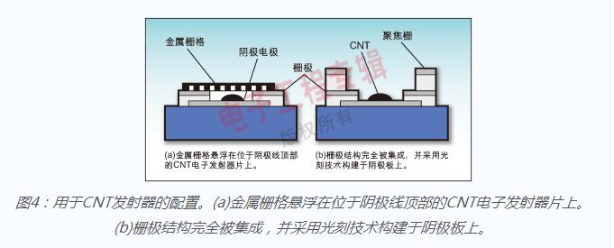
The electron flow of the FED emitter is controlled by the electric field applied on the emitter (caused by the cathode-to-gate bias voltage) and is constrained by the Fowler-Nordheim equation. The emitter current is a function of applied voltage and is highly non-linear. Figure 5 shows an example of IV characteristics of a CNT emitter. In addition to the application of the electric field, the emission current also depends on the emitter's work function() and the shape of the emitter. When the work function is reduced, for example by coating an alkali metal, electrons are more easily taken at a lower electric field. When the shape of the emitter becomes sharper, it is also easier to take or take electrons because the local electric field at the top of the emitter will be higher.

There are two main points when considering standard FED technology. First, the configuration is largely vertical. The general grid is placed close to the cathode so that the applied electric field is mostly vertical at the cathode where the CNT emitters are deposited and the electrons emitted from the cathode will reach the anode directly. Some broadening of the electron beam is caused by the application of a transverse component of the electric field, but the design will limit these components as much as possible, or if necessary, place additional focusing electrodes in the path to correct. Normally, the goal of the FED designer is to prohibit electrons from striking the surface of any surface other than the anode after leaving the emitter.
Second, a typical FED is a voltage-driven device. In a passive-matrix FED display, it is difficult to apply more than two or three voltage levels between the cathode and the gate (on and off voltages), so the gray scale of the image is achieved by pulse width modulation. For all passive-matrix flat-panel displays, the image is built up on one line. When a row is activated, the pixels of the row are opened by the column driver; the time that each pixel of the row is left open depends on the required luminous intensity of the pixels of the image frame. Because the transmitter's emission current is highly non-linear, the emitter's manufacturing is difficult to control, so the emission and image consistency for the micro-end and CNT display is a big problem to overcome. Manufacturing techniques have improved the consistency of CNT-based FEDs. The emission uniformity of the cathode is usually controlled by a current feedback resistor connected in series with the cathode.
The manufacture of FED emitters depends on the method used by the FED development team. The processes developed by Motorola and LETI require CNTs to grow directly on the cathode substrate, while processes developed by companies such as ANI and Samsung allow CNT printing. Compared with the high-temperature CVD method required for direct CNT growth, the printing method is more suitable for mass production of large-area cathodes with uniform emission performance. The printing method requires an activation step, but even this step is optimized for a large area manufacturing process using bead-blasting techniques.
2, SED structure
The uniqueness of the SED structure compared to other FED technologies is that the electron beam current provided to the anode for each pixel needs to be generated in two steps.
a. step 1
The electron source emits electrons transversely across the very narrow gap formed between the two electrodes. Although the gap between the electrodes is small, only a few nanometers in size, it is still a vacuum gap. It is necessary to apply a certain potential to extract electrons from one electrode and pass through the vacuum tunnel barrier to reach the other electrode. The flow of electrons across the electrode gap follows Fowler-Nordheim's law and is therefore highly non-linear, allowing the matrix-addressable approach to be discussed later. The surface conduction emitter (SCE) comes from this lateral emitter structure. Figure 6 is a block diagram of an SED emitter.
b. Step 2
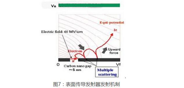
Electrons that pass through the gap and strike the opposite electrode are either absorbed into the opposite electrode (thus generating only heat, not emitting light), or are scattered out, trapped by the electric field established by the anode potential, and accelerate the impact of a precise point of fluorescence, resulting in Red, green or blue dots. This combined electron emission plus electron beam scattering process is shown in Figure 7, where Va represents the anode potential and Vf is the driving potential across the gap. Many scattering events may occur before electrons are captured by the anodic field. Therefore the efficiency of the number of electrons captured by the anode (Ie/If, Fig. 7) is very low, about 3%, but the efficiency is ideal because the Vf is relatively low, about 20V. It is worth noting that the uniformity of the electron flow to the anode depends on the electric field emission current at the gap and the pixel-to-pixel scattering event efficiency.
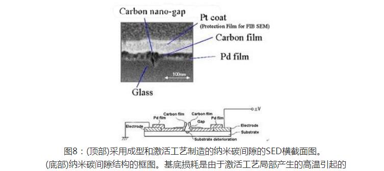
The above emitters are manufactured using a variety of techniques. Simple matrix lines are deposited by printing methods using silver lines and insulating films at the intersections. The platinum (Pt) electrode is made by thin film lithography, and the gap between these electrodes is 60 nm. The nanocarbon gap was created using a two-step process. The PtO film (10nm thick) was first deposited on the Pt electrode and between the electrodes by inkjet printing. This film consists of ultra-fine PdO particles approximately 10 nm in diameter. Then the first step is to apply a series of voltage pulses to the PdO film between the two Pt electrodes to "form" a gap on the film by reducing the oxide layer. Because the substrate is in a vacuum, pulse heat reduces PdO. With the decrease of PdO, the film will be under a certain pressure, eventually forming sub-micrometer gaps within the diameter of the PdO point.
Then, the cathode is exposed to organic gas to "activate" the gap and apply more pulse voltage to the gap. These pulsed voltages will create partial discharges and cause the deposition of CVD-like carbon films in the gaps, and the final gap will shrink to a self-limiting distance of 5 nm. When the gap is large, because the hydrocarbon molecules are in the plasma zone formed by the discharge? ? And deposited carbon. As the gap becomes smaller, the partial discharge current generated by the pulse will increase and the material will gradually evaporate. When the gap is 5 nm, the deposition and evaporation of carbon are balanced. The width of this gap is controlled by the organic gas pressure and pulse voltage. The cross-sectional image of the gap is shown in Figure 8.
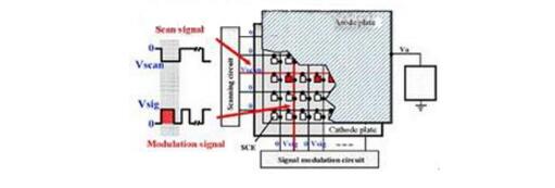
Similar to the FED, SED is also driven line by line, as shown in Figure 9. The scanning circuit generates a scan signal (Vscan), and the signal modulation circuit generates a pulse width modulation signal (Vsig) synchronized with the scan signal. Because surface-conduction transmitters have highly nonlinear Ie-If characteristics, each pixel can be selectively driven without using active cells using a simple matrix xy configuration with a signal voltage of 18.9V and a scan voltage of 9.5V. Still can get 100000:1 brightness contrast. In contrast, the typical signal voltage of a CNT-based FED structure is 35 "50V and the scan voltage is 50" 100V. SED switching devices have much lower voltages, but they must be designed for higher steady state current loads. Due to the low efficiency of the SCE electron scattering mechanism, the maximum current can reach 30 times. The large current of the SED also requires that the interconnect impedance be lower than the FED because even a small voltage drop on the line can lead to edge-to-edge inconsistencies.
Guangzhou Yunge Tianhong Electronic Technology Co., Ltd , https://www.e-cigarettesfactory.com
