Test challenges in the life cycle of power semiconductors
Various testing and characterization activities are required throughout the life cycle of a power semiconductor device. At every stage of the process, engineers face different measurement challenges, from the early design stages of new power devices, to diagnosing faults and ultimately bringing devices to market.
In many cases, engineers have found that their education, training and career paths lead themselves to very narrow areas of expertise. Although they can accumulate expert knowledge in one or two areas, they rarely understand the testing and characterization challenges that peers face in other areas of the product development cycle. They sometimes need to work with other engineers, and when they get out of the comfort zone, there are a lot of problems due to the lack of understanding of these challenges.
Let us look at the challenges involved in the life cycle of power semiconductors from a test and characterization perspective.
Evaluate existing devices for new applicationsApplication engineers work with customers who constantly stress test the design or extend the design for maximum efficiency. These customers require details beyond the device's technical data. Their requirements are constantly changing, so the items to be measured may change every day. How can I make measurements quickly and easily without wasting time re-learning software or instruments?
A very important point for this type of application is to have a full set of test functions, including pulse, DC and CV. Software that uses device-specific vocabulary (rather than instrument-specific vocabulary) can help simplify measurements. The software also simplifies the interaction between multiple source measurement unit (SMU) instruments, allowing users to focus on the device under test rather than on the measuring instrument.
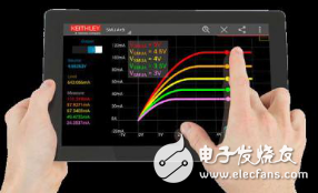
To make things easier, vendors are beginning to offer smartphone and tablet applications for SMU instruments (Figure 1) to perform IV characterization, including 2- and 3-terminal device testing and trend monitoring. These applications can interactively analyze and view device features without the need for programming. Applications include current versus voltage (IV) testing on a variety of materials, 2-terminal and multi-terminal semiconductor devices, solar cells and embedded systems.

Figure 1. The IVy Android application works with Keithley SMUs to perform IV characterization.
Designing devices for changing needsTo effectively design a device that meets the customer's latest requirements, power device design engineers and process engineers must understand how to adjust the process to achieve the desired device performance. They must believe that the device model is sufficiently accurate that changing the specific process steps must produce the necessary changes in the device measurement parameters. Therefore, device engineers must perform a preliminary test on critical device parameters.
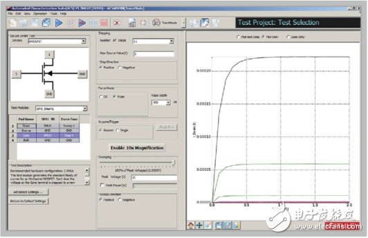
To help bring fully optimized devices to market in less time, parametric plotters are now equipped with software to quickly verify key device parameters and device characteristics, including real-time tracking mode (Figure 2), to check basic device parameters. , such as breakdown voltage; comprehensive parameter mode, extract accurate device parameters. In addition to intuitive operation, these tools include a large library of devices and built-in formula tools to quickly correlate measurements with device parameters.

Figure 2. Tracking mode provides a comprehensive representation of the device.
Characterization performanceThe characterization engineer provides the necessary professional measurement knowledge and understands how measurement anomalies can affect non-target areas of device performance. Results must be obtained quickly so that the device engineer or process engineer can repeatedly manipulate the measurement data to quickly convert to device parameters.
Measuring the DC and capacitance parameters of high power semiconductor devices requires sufficient expertise to optimize the accuracy of various measurements. Even for engineers with this expertise, managing changes in settings between open state, point state, and capacitance-voltage (CV) measurements can be time consuming and error prone.
These challenges are especially tricky in a wafer environment. The characteristic curve of a power transistor, FET or diode includes its typical output characteristics. Some power devices may have output characteristics ranging from tens to hundreds of amps. Therefore, creating these curves requires high-flow instruments such as SMU (Source Measurement Unit). When multiple SMUs are configured in parallel, they generate up to 100A of pulsed current, which creates challenges in managing cable resistance and inductance to ensure accurate results.
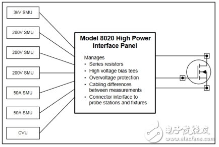
To reduce the problems encountered when performing full DC IV and CV testing of power semiconductor devices, many engineers use high-power interface panels (Figure 3) to minimize connection variations between major measurement types. IV and CV measurements can be made with T-type bias without changing the connection, reducing the chance of user error.

Figure 3. The high-power interface panel addresses the connectivity challenges of wafer device testing.
[Video content:]
Model 8020 High Power Interface Panel: Model 8020 High Power Interface Panel
Manages: Management
Series resistors: series resistors
High voltage bias tees: High voltage T-type bias
Overvoltage protecTIon: Overvoltage protection
Cabling differences between measurements: Cable differences between measurements
Connector interface to probe staTIons and fixtures: connector to probe station and fixture interface
The device is ready for productionIn order for the device to be properly put into production, the production test engineer must demonstrate the ability to reliably produce the device. Measurement data must be collected to obtain statistical results of the device's technical data; the test time must be optimized to meet the required production throughput. For these applications, multi-function instruments provide the best way to quickly obtain measurement data and minimize connection changes and switches.
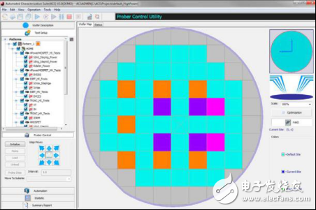
SMUs are multi-function instruments that have been proven to be used in semiconductor applications. SMU instruments with increased test scripts can improve throughput because they enable tight synchronization, built-in complex arithmetic processors, and decision making within the instrument to minimize communication time. SMUs instruments can be used in parametric curve diagram configurations for interactive testing and automated production testing. It offers automated software (Figure 4) that combines advanced semiconductor test capabilities with control, data reporting and statistics.

Figure 4. Test software maps devices and tests to sites and substations without having to repeat each test for each substation, reducing test development time.
Meet reliability standardsTo determine that a device meets commercial reliability standards, reliability test engineers have multiple responsibilities:
· Determine if the device can withstand environmental stress and continue to meet specifications
· Answer customer-related issues related to the device life cycle (MTBF, MTTF)
· Provide critical information to determine if the device is suitable for specific high reliability applications, including military/defense, aerospace, and automotive
Creating statistically relevant results requires an adequate number of test device samples. Pressure measurement of multiple devices requires multi-channel parallel testing and automatic evaluation of data.
Integrated test systems are typically used for this type of application and can be customized to suit a variety of application environments. These systems use software controls to cycle pressure measurements and make comprehensive decisions. There are a variety of power and SMU instrumentation solutions on the market that can power and test any number of devices simultaneously.
Implement the device in the actual design
Once the device is verified, it is ready for commercial use. The user must verify that the device is within the tolerances of the application to ensure that the final product achieves the expected power efficiency. As devices mature and are available from multiple vendors, power device consumers need to quickly detect the devices they acquire, identify and eliminate counterfeit products, and avoid potential problems in the final product.
The test instruments used at this time are: a programmable power supply for powering the basic board, a power analyzer, an oscilloscope equipped with a power analysis module and a high voltage probe, a current probe, and a differential probe. A power analyzer is used to evaluate the performance of the entire final product. The oscilloscope can analyze switching losses, harmonics, and safe operating areas.
Diagnosing device failure
The failure analysis engineer must determine if the failure was caused by the use of the final product or by a design problem that was previously missed. Once this decision is made, the cause of the failure must be known in the design and process engineering so that process changes or design changes can be implemented to prevent future failures.
It is important to be able to quickly measure device technical data, including static data and dynamic data. To mimic the final application to reproduce the fault. A parametric graph plotter with tracking mode can perform this type of analysis. Software tools with built-in stress test measurements can reproduce conditions that degrade device performance.
summary From start to finish, testing and measurement play an important role in bringing new power semiconductor devices to market and adapting them to customer applications. Understanding the entire product development cycle and testing challenges at each stage helps ensure that the entire design process runs smoothly.
This article is selected from the electronic enthusiasts August theme month technical feed, please indicate the source
About the author of this article

Wilson Lee is currently Senior Marketing Manager at Tektronix Technologies. Prior to joining Tektronix Technologies, Wilson had more than 25 years of professional experience, including technical market and technical sales executives, such as CTS Electronic Components, and other technology/value-added resellers such as Richardson RFPD and Premier Farnell. Wilson has been focusing on design work within the market segments of RF/wireless, industrial power supply, and industrial automation.
Wilson earned a Bachelor of Science degree from Cornell University. While living in New York, Chicago and Asia during his career, he currently lives in Portland, Oregon, USA.
Tovapo Vape is so convenient, portable, and small volume, you just need to take them out of your pocket and take a puff,
feel the cloud of smoke, and the fragrance of fruit surrounding you. It's so great.
We are China leading manufacturer and supplier of Disposable Vapes puff bars, Tovapo vape pen,Tovapo disposable vape,Tovapo e cig,
Tovapo vape kit, and e-cigarette kit, and we specialize in disposable vapes, e-cigarette vape pens, e-cigarette kits, etc.
Tovapo vape pen,Tovapo disposable vape,Tovapo e cig,Tovapo vape kit,Tovapo e-cigarette
Ningbo Autrends International Trade Co.,Ltd. , https://www.mosvape.com
