A new generation of high-brightness LEDs can be fabricated with proximity exposure devices
Recently, SUSS MicroTec AG disclosed that the approximately 3 μm pattern required for the manufacture of a new generation of high-brightness LEDs can be resolved using existing proximity exposure devices. This is achieved by improving the optical system and illumination of the proximity exposure device, and changing the photomask. With this technology, LED manufacturers are expected to use proximity exposure devices in the development and mass production of next-generation high-brightness LEDs without the need to introduce expensive projection exposure devices such as steppers.
The company is a large-scale manufacturer of proximity exposure devices for MEMS, semiconductor packaging and LEDs. Although the relevant content has not been announced, Tech-On!'s interview shows that among the large LED manufacturers, it is estimated that each company uses dozens to 100 Sussex exposure devices.
A new generation of high-brightness LED manufacturing requires a pattern of about 3 μm in order to prepare a structure that can improve the light extraction efficiency of LEDs on a substrate such as sapphire. This structure needs to be periodically formed in a size of 3 to 4 μm.
The proximity exposure apparatus used in the conventional LED structure cannot form a pattern of about 3 μm. Therefore, it is generally believed in the industry that a projection exposure device such as a stepper is required for mass production of a new generation of high-brightness LEDs.
In an exposure technique capable of achieving a resolution of about 3 μm, in addition to projection exposure, vacuum contact exposure is also available. This is a technique in which a vacuum state is formed between the photo-curing mold and the bottom plate, so that the distance between the two is narrower than the proximity exposure, thereby improving the resolution. However, vacuum contact exposure has a problem of low yield, and it is recognized that it is difficult to use for mass production.
An example of a 2.5 μm square pattern formed. The exposure gap between the photomask and the substrate was 100 μm. There is less passivation in the angular portion. Provided by Suss Micro.
An example of a hexagonal pattern of 5 μm or less formed. The exposure gap was 40 μm. Provided by Suss Micro.
SMO for proximity exposure
Suss Micro disclosed that through the three improvements, a 2.5μm pattern can be formed by using a proximity exposure device: (1) optimization of an optical system such as a new microlens; (2) additional filter optimization lighting system; 3) OPC (Optical Proximity Correction) technology is applied to the photomask. (1) and (2) can be achieved by modifying existing exposure devices. By combining these three improvements, the same SMO (Source Mask Optimization) as the optimization method of the entire exposure process of the cutting-edge semiconductor device is realized.
The optical system improvement in (1) is intended to make the illumination characteristics of the light source more stable. The new microlens array, which can reduce the illumination deviation, can improve the intensity and angular uniformity of the illumination light, and can also eliminate the poor optical factors that cause the light source to be misaligned and the brightness of the light-emitting surface to be uneven.
The lighting system improvement in (2) aims to control the illumination light with high precision. By inserting a filter for illumination, high precision of illumination light is achieved.
(3) OPC is added to prevent image failure and process failure that may occur when pattern exposure of about 3 μm is performed by only the above (1) and (2). As with the OPC for memory and logic LSI, an auxiliary pattern below the image boundary is additionally added to the photomask pattern.
According to the company, when the proximity exposure of about 3 μm is performed by only (1) and (2), the shadow of the Cr pattern formed on the photo-baking mold is easily transferred to the photoresist, and the corner portion of the pattern is passivated. , line width chaos, line end defects, and areas with different pattern densities produce shape confusion due to proximity effects, and so on. (Editor: maysoong)

ZGAR MINI
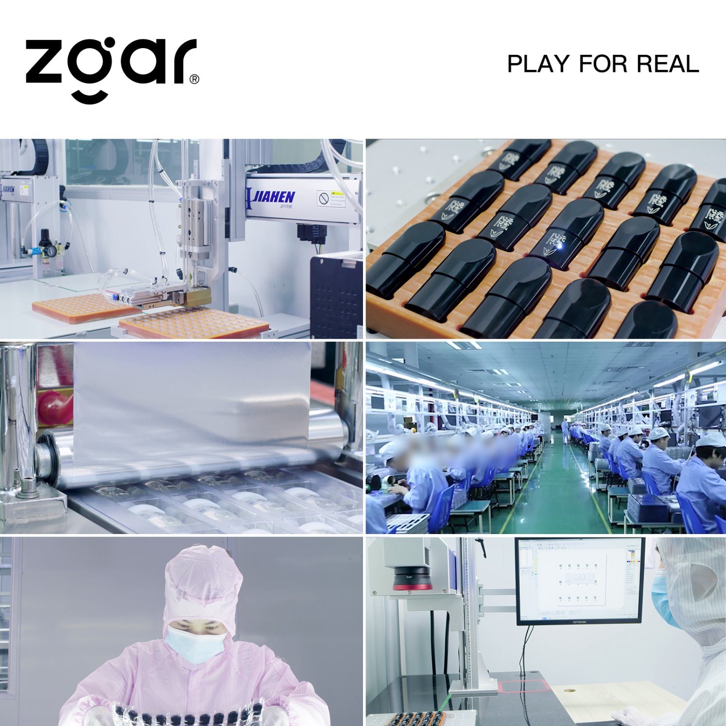
ZGAR electronic cigarette uses high-tech R&D, food grade disposable pod device and high-quality raw material. All package designs are Original IP. Our designer team is from Hong Kong. We have very high requirements for product quality, flavors taste and packaging design. The E-liquid is imported, materials are food grade, and assembly plant is medical-grade dust-free workshops.
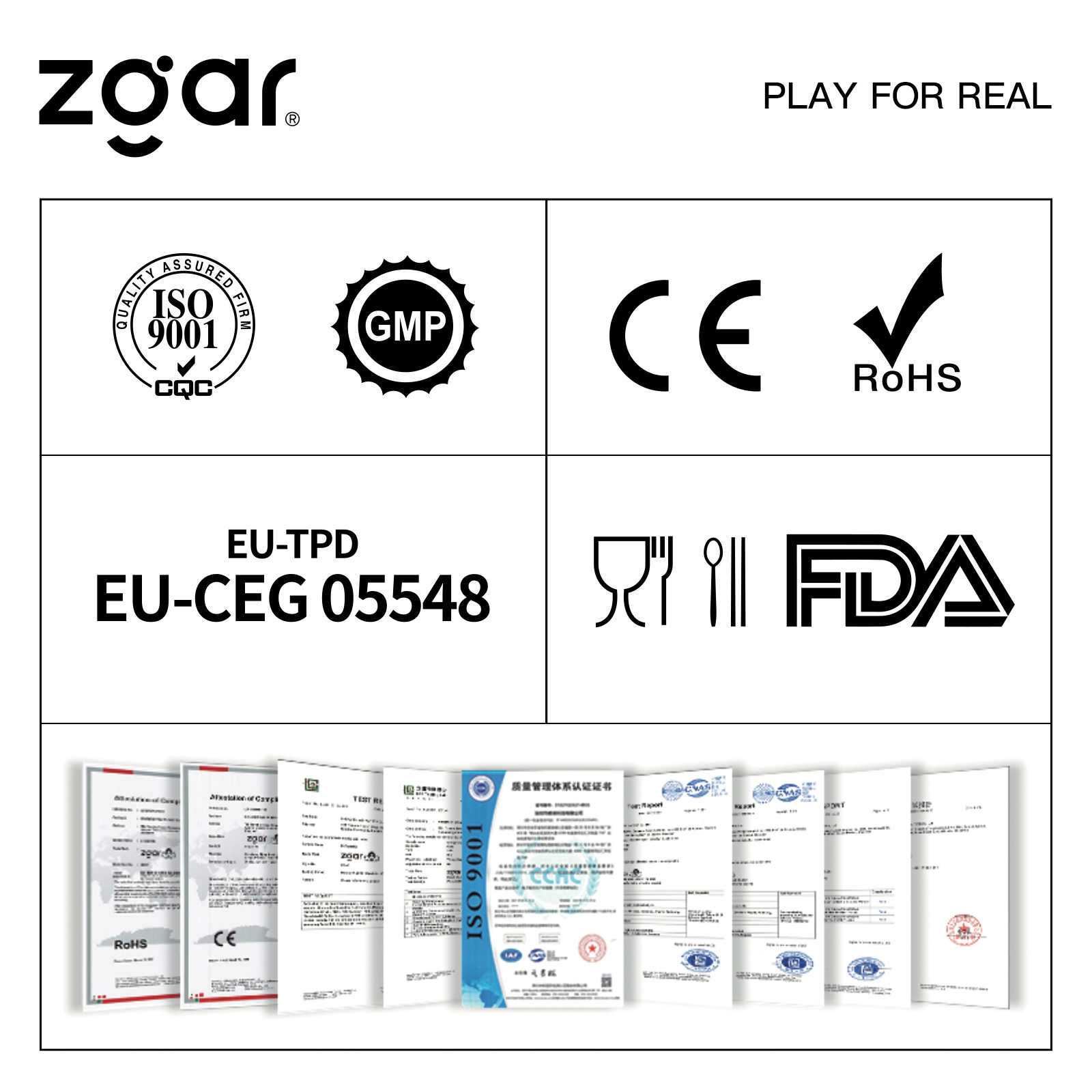
From production to packaging, the whole system of tracking, efficient and orderly process, achieving daily efficient output. We pay attention to the details of each process control. The first class dust-free production workshop has passed the GMP food and drug production standard certification, ensuring quality and safety. We choose the products with a traceability system, which can not only effectively track and trace all kinds of data, but also ensure good product quality.
We offer best price, high quality Vape Device, E-Cigarette Vape Pen, Disposable Device Vape,Vape Pen Atomizer, Electronic cigarette to all over the world.
Much Better Vaping Experience!


ZGAR Vape Pen,Disposable Device Vape Pen,UK ZGAR MINI Wholesale,ZGAR MINI Disposable E-Cigarette OEM Vape Pen,ODM/OEM electronic cigarette,ZGAR Mini Device
Zgar International (M) SDN BHD , https://www.zgarette.com
