Adc0809 working principle diagram and program flow chart
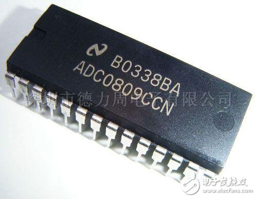
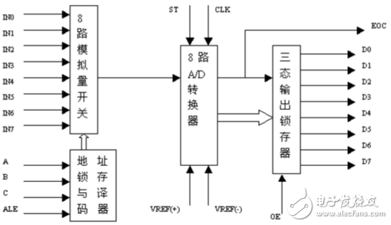
Adc0809 is a CMOS process 8-channel, 8-bit successive approximation A/D analog-to-digital converter manufactured by National Semiconductor. It has an 8-channel multiplexer inside, which can latch the decoded signal according to the address code and only strobe one of the 8 analog input signals for A/D conversion. At present, it is only common in the application design of single-chip microcomputer.

Adc0809 requirements for input analog: signal unipolar, voltage range is 0-5V, if the signal is too small, it must be amplified; the input analog quantity should remain unchanged during the conversion process, if the analog quantity changes too fast, then Increase the sample and hold circuit before input.
Address input and control line: 4
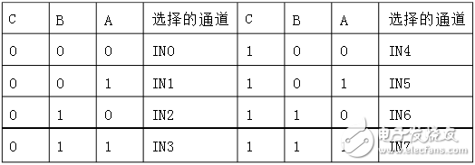
ALE is the address latch enable input line, active high. When the ALE line is high, the address latch and the decoder latch the address signals of the three address lines A, B, and C, and the analog signals of the selected channel are converted into converters after being decoded. A, B and C are address input lines for strobing an analog input on IN0-IN7. The channel selection table is shown in the table below.

Digital output and control line: 11
ST is the conversion start signal. When the ST edge is skipped, all internal registers are cleared; when the next edge is skipped, A/D conversion is started; during the conversion, ST should be held low. EOC is the end of conversion signal. When EOC is high, it indicates the end of the conversion; otherwise, it indicates that A/D conversion is in progress. OE is an output enable signal for controlling the data output from the three output latches to the microcontroller output. OE=1, output converted data; OE=0, the output data line is in a high impedance state. D7-D0 is a digital output line.
CLK is the clock input signal line. Since there is no clock circuit inside the adc0809, the required clock signal must be provided by the outside world, usually using a frequency of 500KHZ.
VREF(+), VREF(-) are reference voltage inputs.
Adc0809 application note
(1) adc0809 has an internal output latch that can be directly connected to the AT89S51 microcontroller.
(2) When initializing, make the ST and OE signals all low.
(3) Which address of the channel to be converted is sent to the A, B, and C ports.
(4) A positive pulse signal of at least 100 ns wide is given at the ST end.
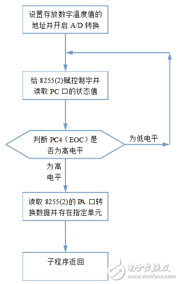
(5) Whether the conversion is completed, we judge according to the EOC signal.
(6) When EOC goes high, then OE is high, and the converted data is output to the microcontroller.
The startup mode of AD0809 is pulse start mode. The start signal starts to start after START start, and the EOC signal becomes invalid low level after 10us of the falling edge of START. This requires the query program to start the query after the EOC is invalid. After the conversion is completed, the EOC outputs a high level, and then the OE goes high to output the converted data. We can use the EOC signal to inform the microcontroller (query method or interrupt method) to read the converted data when designing the program. It can also read the converted data after starting AD0809 with appropriate delay.
Adc0809 program flow chart
Brushed Stainless Steel Plate,Hot Rolled Brushed Stainless Steel Plates,Dimple Plate Stainless Steel,Professinal Dimple Plate Stainless Steel
ShenZhen Haofa Metal Precision Parts Technology Co., Ltd. , https://www.haofametals.com
