Design of Grating Demodulation System Based on FPGA
Abstract: The sensing information of fiber grating is carried out by wavelength coding. The key to demodulation is to completely demodulate the sensing information from wavelength coding. The grating demodulation system introduced in this paper uses F-P filter to scan the ASE source; FPGA is used as the control core; DM9000A is used to complete the network interface design, and the program design of the grating sensing signal centroid demodulation algorithm is implemented in the FPGA. The design of the Ethernet interface control program, the FPGA has the ability of multi-channel high-speed synchronous solution, and realizes the synchronous real-time solution of the fiber grating wavelength under the scanning rate of 500 Hz of the F-P filter. The demodulation system's demodulation accuracy can reach about 2 pm.
0 PrefaceAmong all kinds of fiber Bragg grating sensors, quasi-distributed fiber Bragg grating (FBG) transmitter arrays are the most widely used, and their characteristics are mainly measured by the center wavelength of reflected light (Bragg wavelength), which is not affected by source power fluctuation and fiber microbend effect. And the influence of factors such as coupling loss. As a wavelength modulation type sensor, the fiber Bragg grating converts the measured information into the center wavelength of the Bragg grating. By demodulating the center wavelength drift from the measured optical signal, the measurement of the measured information can be realized. At present, the most commonly used methods for detecting the small change of the grating wavelength with the measured physical quantity of the outside world include the edge filter method, the tunable filter method, and the demodulation method based on the tunable semiconductor laser or the scanning fiber laser, etc., signal processing The method includes direct comparison method, centroid method (also called power weighting method), Gaussian fitting method, etc., as well as demodulation methods combined with digital filtering [1]. Design a grating sensing system based on scanning fiber laser design, use the 12-bit A/D acquisition module to acquire the signal into the computer, realize the centroid signal processing through the high-performance FPGA programmable device, and then solve the result through the network port. Output to the PC and display it.
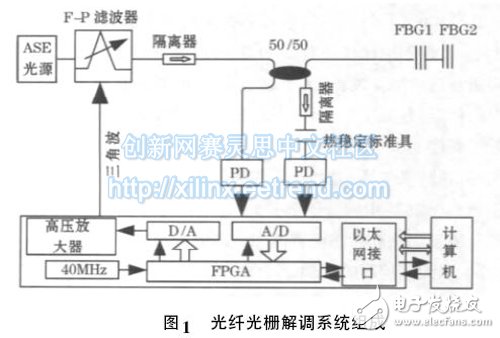
1 overall system designThe fiber Bragg grating demodulation system is mainly composed of the sensing optical path and the FPGA acquisition and processing circuit 2, as shown in Figure 1.

Its main working principle: Under the driving of the sawtooth wave and ASE light source generated by the FPGA control board, the scanning fiber laser composed of F-P filter emits laser light, and the laser wavelength is scanned by adding the original triangular wave control D by the FPGA. /A output high voltage triangular wave implementation. The output light is divided into 2 parts by fiber coupler, 1 part is used for real-time calibration, real-time calibration of scanning laser wavelength is realized by FP etalon with wavelength mark [2], the wavelength repeatability is guaranteed, and the output light is directly connected. Photodetector (PD); 1 part for grating demodulation channels. In the grating demodulation channel, the reflected light of the sensing grating is coupled to the PD. The signals output by each detector are quantized by the A/D converter and directly processed by the centroid demodulation algorithm by the FPGA. The processed data is then transmitted to the computer through the Ethernet interface for further solution, storage and display.
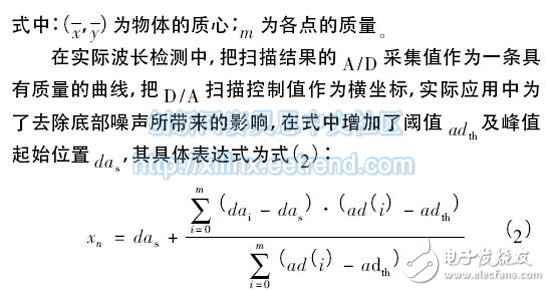
2 centroid method wavelength detection principleThe centroid principle [3] is derived from the principle of torque balance, that is, the moment produced by the mass of each point of a uniform density object on a certain axis, equal to the moment generated by the mass of all the masses concentrated at a specific position. The specific position is the centroid of the object and can be expressed as (1):


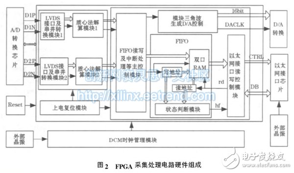
The hardware composition of the FPGA acquisition processing circuit is shown in Figure 2.
In the figure, the PGA hardware circuit mainly completes the processing of the LVDS interface, the implementation of the algorithm, the control of the FIFO, the processing of the clock management module, the generation of the triangular wave signal, and the control of the Ethernet. The FPGA control and solution module is an important part of the design, which controls the centroid resolution of the signal, Ethernet interface and so on.

Pc Power Supply,Gold Pc Power Supply,Desktop Power Supply 650W,Psu Computer Power
Boluo Xurong Electronics Co., Ltd. , https://www.greenleaf-pc.com
