Implementation and Optimization of Embedded Video Image System Compression Algorithm
introduction
This article refers to the address: http://
With the development of network technology and multimedia technology, the demand for video communication is gradually increasing. At the same time, the latest video compression standards are continuously introduced. MPEG-4 (Moving Pictures Expcrts Group-4) was developed by the MPEG Moving Picture Experts Group in November 1998 [1], which is different from other standards. It is a compression for multimedia applications. Standard. The first object-based compression method was proposed. This makes it possible to implement interactive functions. Recently, the MPEG-4 video encoder based on PC platform [2] has been applied in remote education and high-definition movies on the Internet, but it is more widely used in embedded systems such as DVR and multimedia communication. widely. The system with DSP as the core of embedded image processing has the characteristics of short development cycle and flexible programming. Therefore, DSP image processing system has become a research hotspot.
DSPs structure features
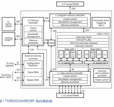
TMS320C6455 is the latest high-speed DSP chip introduced by TI (Tcxas Instrumcnts Incorporatcd) [3]. The specific structure is shown in Figure 1. The main feature is that the structure [4] uses the VLIW (VLIW: VeryLong Instruction Word) super long instruction word kernel structure. With a CPU of 1200 MHz, eight 32-bit instructions can be executed simultaneously in each cycle. Speeds up to 9600 MIPS (1200 MHz X 8 instructions = 4 800 MIPS). The on-chip uses a 2-level cache structure. The off-chip memory has a very powerful external memory interface EMIF (Extcrnal Mcm ory Intcrfacc). These capabilities meet the real-time requirements of video image processing and establish its position in high-end multimedia applications.

Figure 1 Kernel structure of TMS320C6455DSP
Optimization of Cache
Maximizing Cache efficiency is a key factor in achieving the desired encoder performance [5]. Cache's high-speed storage access speed reduces CPU latency and improves processor efficiency. The TMS320C64xDSP has two levels of memory structure for on-chip data and program storage. For L1Cache it can be accessed at the same speed as the CPU. L2Cache can be used both as data space and as program space. L2 is a bridge between off-chip space and L1.
The MPEG-4 video encoder performs encoding processing in units of macroblocks, and the video encoder can transmit a macroblock only after the current macroblock processing completes all the processes. The shortcomings that appear directly are: The entire code of a video encoder is larger than L1P. The transfer process between each macroblock between L1P and L2 results in a serious Cache miss. The movement of a single macroblock from the off-chip memory space to the on-chip space does not take advantage of EDMA (Extended Direct Memony Access).
In order to avoid a large number of Cache missing, three methods are adopted [6].
1. The entire coding algorithm should be divided into three modules: macroblock coding, motion estimation, motion reconstruction, so that each module code is suitable for L1P. Each cycle is in units of macroblock groups, and the size of the macroblock group is determined by the L1D size. In the macroblock coding module, when macroblock groups are transmitted to the on-chip, they are subjected to DCT Direct Cosine Transform, quantization, and entropy coding together, and L1D refreshes the macroblocks until the macroblock group coding module ends. At the same time, the corresponding programs including DCT, quantization, and entropy coding are also saved to L1P.
2. Minimize the size of the data type. You can use 8-bit data instead of 16-bit data, which not only saves space, but also improves the efficiency of L1D. Because the size of the L1D line is fixed, if 8-bit data is used in one row, it can be doubled compared to 16-bit data, thereby reducing the occurrence of Cache miss in the program.
3. Adopt ping-pong cache structure to improve cache hit rate and reduce CPU wait time.
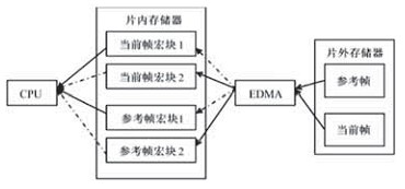
In the video coding module, the current frame and the reference frame data are placed in an off-chip memory, and each macroblock in the image frame needs to be sequentially operated during the encoding process. However, the macro block is read directly from off-chip memory, which causes CPU wait. Two pairs of on-chip buffers can be set, one pair stores the current frame macroblock, and one pair stores reference frame macroblocks, which work in ping-pong mode. The ping-pong buffer working mode is shown in Figure 1. The pre-encoding E DMA moves the coded macroblock data in the current frame outside the slice and the reference frame macroblock data in the search range to the on-chip memory. While EDMA is used to move data to one of the on-chip caches, the processor can process the data in another block. After such modification, the CPU has been reading the memory data from the chip to greatly reduce the occurrence of CPU blocking and improve the encoding speed.

Figure 2 Ping Pong buffer memory structure
Optimization of SAD and pixel interpolation
The SAD (Sum of Absolute Difference) is the key module of the motion estimation module [7], and the DM642 provides a rich set of video and image specific instructions to efficiently implement the motion estimation algorithm.
The LDNDW (Load Non2alignedDoubleWord) instruction can read 64-bit unbounded data at a time. This instruction can read eight 8-bit pixel data at a time from the current frame and the reference frame. Therefore, the moving speed of the current frame and the reference frame macroblock data can be improved.
The SUBABS4 (Subtractwith Absolute) instruction calculates the difference between the four absolute values ​​between the two sets of 8-bit data packets.
DOPTPU4 is an operation that computes the sum of 4 pairs of 8-bit data products. The two DOPTPU4s can be paralleled in a single cycle, so the calculation speed of the SAD can be greatly improved. Specific steps are as follows:
1) Two LDNDW instructions take 8 pixels from the current frame and the reference frame;
2) Two SUBABS4 calculate the difference of 8 pixels;
3) Two DOTPU4 calculate the summation of 8 pixel products.
Pixel interpolation is also a computationally intensive module. The AVG4 instruction can perform four 8-bit numerical average calculations. AVG2 can perform an average calculation of two 16-bit data. SHRMB (Shift Right and Merge Byte) Shifts the second register to the right and the lower register of the first register as the high byte. AVG4 calculates the average and SHRMB processes the results.
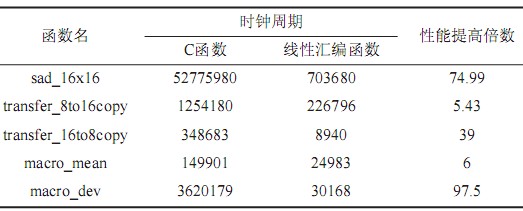
In addition, the author refers to the IMGLIB support library provided by TI. The library also includes many commonly used image and video processing functions to complete functions such as DCT, IDCT (Inverse Direct Cosine Transform), median filtering, etc. These functions are optimized by assembly. . It is fully capable of implementing software pipelines and is highly efficient. The standard sequence Coastguard.yuv is used to encode 5 frames of data, and the performance comparison of the main functions before and after optimization is shown in Table 1.
Table 1 Comparison of optimization performance of each function

Tab1Performance of functions by analysis
Use EDMA for data movement to increase storage speed
The TMS320C6455 DSP supports the EDMA function, which is a way of accessing the memory without CPU intervention. It can directly move data from peripherals or off-chip memory directly to on-chip memory directly through the EDMA channel. For the CPU, the accessed data is always on-chip, no blocking occurs, reducing CPU latency [8].
Use TI's CSL (Chip SupportLibrary) support function [9,10]. It has a dedicated DMA module that facilitates individual memory control of the DMA. The DAT function is mainly used to perform data transfer between DMA memories. This uses DAT copy ( ) and DAT fill ( ).
Just like the common memory operations memcpy and memset, you only need to indicate the source address, destination address, length, dimension attribute, etc. in the API interface, and you don't need to consider the specific registers.
The following code is to move a frame in a 90-frame CIF 288 × 352 format video sequence in SDRAM using EDMA in the cache.
DAT_open(DAT_CHANNY, DAT_ PRI_ LOW, DAT_OPEN_2D);
Copy2FrameBuf(Unit8*framebuf)
{
If((tempbuf_rawbuf)>13685852)
If (tempbuf!=NULL)
Free(tempbuf);
Return 1;
}
DAT.copy(tempbuf,framebuf,152064);
Tembuf+=152064;
Return 0;
}
Overall performance of the encoder
Table 2 MPEG-4 encoder performance

It can be seen from the data in Table 2 that the frame rate of different video sequences is increased by at least 5 times, although the signal-to-noise ratio is reduced, but the frequency frame is greatly improved and real-time requirements are obtained, and the display effect is better.
Conclusion
The author discusses the measures for optimizing the video coding algorithm on the TMS32OC6455DSP platform. The main consideration is to optimize according to the characteristics of DSP and video algorithm. It can verify the real-time requirements of more than 30 frames/second through experiments. With the development of IC technology and the reduction of DSP price, the commercial value of DSP-based video encoders is coming. The more obvious.
Dc Relay,Dc Power Relay,Condenser Contactor,Voltage Protection Relay
NanJing QUANNING electric Co.,Ltd , https://www.quanningtrading.com
