Introduction to the structural design and working principle of the voltage regulator circuit
In recent years, with the development of wireless communication technology and microelectronics technology, non-contact IC card (radio frequency card) technology has flourished and has been rapidly popularized and promoted in many fields, such as bus automatic ticketing system and resident ID card. Card, phone card, *, etc. Passive power supply technology is one of the key technologies of RF cards. At present, it is mainly solved by the principle of electromagnetic induction and integrated voltage regulator circuit. When the RF card enters the magnetic field of the reader, energy is obtained from the magnetic field by electromagnetic induction, that is, an alternating current is induced at both ends of the coil of the card, and a DC voltage is obtained after rectification and voltage regulation. This article discusses a self-feedback switching regulator circuit designed for RF cards using a 0.35um CMOS process.
2. Structure design and working principle of voltage regulator circuitThe integrated voltage regulator circuit is also called an integrated voltage regulator. When the input voltage or output current changes within a certain range, the output voltage remains unchanged. It has been widely used in a variety of electronic equipment to replace the regulated power supply assembled by discrete devices.
2.1 Circuit structure design
The integrated voltage stabilizing circuit mainly includes the following parts: a reference source circuit, a voltage regulating circuit and a power switch circuit.
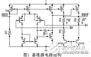
The reference source circuit is composed of a band gap reference source composed of a two-stage CMOS differential amplifying circuit and a transistor circuit. Its structure is shown in Figure 1.

The active resistor P0 and the polycrystalline resistor R7 form a bias circuit that provides a bias current to the circuit. The two inputs of the two-stage differential amplifier are connected at Q1 and Q2. From the reference source principle, the output of the reference source can maintain good performance only when the input offset voltage of the amplifier circuit is small and is not affected by temperature. According to the action of the amplifier and the energy gap reference source principle:
I1R6=I2R4 (1)
It can be seen from equation (1) that the input offset voltage of the amplifier in the circuit is close to zero. Therefore, the voltage value of the REF point after stabilization is as follows:
VREF=VQ1+VR6=VQ1+R6I1= VQ1+R4I2 (2)
Since the base and collector of the PNP transistor are connected, the VQ1 value corresponds to the forward voltage drop VBE of the BE junction diode in the transistor, and VBE is generally 0.6 "0.8V.
The temperature coefficient of the BE junction diode in the transistor is negative, and the temperature coefficient of the resistor is positive. In the equation (2), the changes of VQ1 and VR6 with temperature can compensate each other, so the output VREF of the reference source is insensitive to temperature changes.
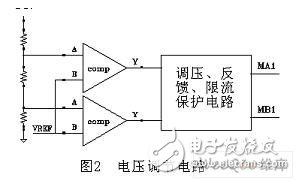
The voltage regulation circuit is the core part of the voltage regulator circuit, including two first-level CMOS differential amplifier circuits COMP and voltage regulation and feedback circuits, as shown in Figure 2.

The input of the two differential amplifiers is obtained by the voltage dividing resistor. After comparison and amplification, the feedback regulation and current limiting protection circuit are used to obtain the opening and closing of the switching tube in the control power switching circuit since MA1 and MB1.
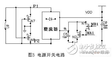
The power switch circuit is composed of a storage capacitor, a rectifier composed of an NMOS transistor, and a switch circuit, as shown in FIG. P1 and P2 are directly connected to the two ends of the coil L0, and an alternating current is induced on P1 and P2 through electromagnetic coupling, and a DC voltage VDD is generated at the C0 end of the storage capacitor after rectification. The voltage regulating capacitor C5 forms a discharge circuit after the N2 tube is turned on, so that the current on P1 and P2 starts to charge C5 and stops charging C0, so that the voltage across C0 remains stable, which provides a stable power supply voltage for the load circuit.

2.2 Working principle:
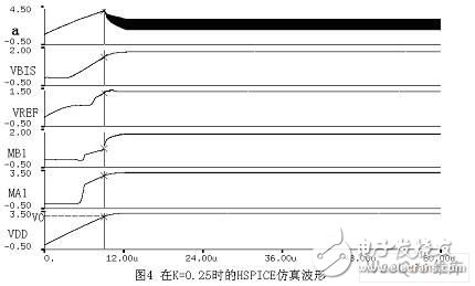
When the RF card enters the magnetic field of the reader, the AC induction current is generated on P1 and P2 through the electromagnetic coupling of the coil, and is converted into a DC current through the rectifier, and simultaneously charges the storage capacitor C0 and the voltage adjustment capacitor C5. The C5 capacitor is very small, and the current through the rectifier can be filled instantaneously. Since the N2 tube is cut off and there is no discharge loop on both sides of C5, the current on P1 and P2 will only charge the capacitor C0, and the power supply voltage VDD is generated across C0. The capacitor charging process continues to rise. The action of the active resistor and the diode in the rectifier causes the voltage amplitude across P1 and P2 to rise, causing the potential at point a to rise. At the same time, the output of the voltage sampling circuit also rises with the increase of VDD. When the VDD voltage value reaches V0 (see Figure 4), the sampling output voltage is greater than the reference voltage VREF. At this time, the output voltage of the MA1 and MB1 in the voltage regulating circuit enables the two tubes N1 and N2 to be turned on successively. Since the source end of the N2 tube is grounded, the voltage on a after the N2 tube is turned on begins to decrease, so that P1 and P2 charge C5 again. Since the N2 tube is always in the on state, C5 also starts to discharge at the same time. Thereafter, the C5 and N2 tubes are always in a state of being discharged while being charged, and the voltage at point a oscillates within a certain range. The charge and discharge of C5 is controlled to keep the voltage peak on P1 and P2 at a certain potential, and the capacitor C0 is no longer charged, so the voltage difference across C0 remains stable. The VDD obtained at this time is the working voltage we need. When the RF card is working normally, the voltage on the storage capacitor C0 will decrease due to the consumption of the load circuit. When the VDD value is less than the V0 value, the N2 tube will be cut off, and the C5 capacitor will not discharge the circuit. After P1 and P2 charge the C5, Continue charging C0 to increase the voltage difference across C0, that is, VDD rises. In this way, a self-feedback regulated power supply is formed in the circuit.

In the normal working environment of the RF card, the coupling coefficient of the card and the reader is generally 0.1"0.35 or so, and the reader signal voltage is generally 12V. In the simulation verification, the test excitation of 12V and 13.56MHz is added to obtain the inductance L0. Inductive current. Using a 0.35um SPICE model, the coupling coefficient is set to 0.25, and the VDD stable voltage is 3.35V. The Hspice simulation results are shown in Figure 4:
4 ConclusionThrough the above design and simulation analysis, it can be known that the voltage regulator circuit can obtain stable voltage in a short time and can be automatically adjusted; the multi-target flow test results are basically consistent with the simulation results and meet the design requirements, so it has good practicability. And reference value.
Shenzhen Guan Chen Electronics Co., Ltd. is a High-tech enterprise that integrates R&D, design, manufacture of computer peripheral products.The products include Thunderbolt Docking Station,USB Docking Station,USB Hubs,USB Adapter, Thunderbolt Cable, SSD Enclosure , HDD Enclosure . Our company adheres to the principle and motto of Being sincere, Responsible, Practical to meet the needs of markets and customers with high quality technology and management. We commit ourselves to new product development and also stress the exploring of international markets.
Our company owns a professional production team and establishes strict quality control standard, so we can provide high quality products and service for customers. We have Grapgic designer,3D Deisnger and Electronic designer to provides professional OEM/ODM service. Our factory covers an area of 1,000-2000 spare meters, which houses 100-200 workers, so our production capacity reaches 50,000 pieces every day.With more than 10 engineers focusing on research and development, our private model attracts much among different markets. Over 100 new designed models are released per year.There are also 3 lean production lines to fullfill small quatity orders production for variety of models.
Our Thunderbolt 3 Docking Station has passed thunderbolt certified by intel and apple.Our product also all can meet with CE, RoHS, UL, FCC and other related certification.And our factory also meets legal environmental standards ensuring your order is delivered. We have a very good reputation at home and abroad. Our products are mainly exported to Europe, USA and Southeast Asia. We provide one-stop-service and promote customers achieve rapidly development. Customer comes First, Quality Ranks First, and Reasonable Price.Guanchen will be your faithful partner from China.
Ngff Ssd Enclosure,M.2 Ngff Ssd Enclosure,Type-C Ngff M.2 External Ssd Enclosure,Ngff External Ssd Enclosure
Shenzhen GuanChen Electronics Co., Ltd. , https://www.gcneotech.com
