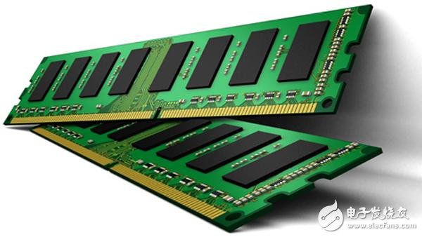
Read the reorder buffer with DDR controller to increase DRAM bandwidth by ten times
Overview
DDR DRAM memory controllers have to meet the needs of many market competition. An excellent memory controller must be able to increase the bandwidth of the memory interface to meet the CPU, graphics processing, system real-time DRAM latency requirements, while meeting the requirements of the memory bus and on-chip bus standards.
The Read Reordering Buffer (RRB) is a silicon-proven architectural enhancement available on the DesignWare uMCTL and uMCTL2 DDR Memory Controller IP products and is a further enhancement to the DDR memory controller architecture. This white paper explains the concept of reading reorder buffers and explains how to increase storage bandwidth. In addition, the paper also summarizes the test results, showing the different architecture of the DRAM controller (according to the controller is RRB, RRB with external scheduling, or RRB with content addressable memory (CAM) scheduling) A very different DRAM bus utilization of 10%, 66% or 100% is obtained from the same input data stream.

Transaction Reordering on DRAM Controllers Each storage subsystem must conform to the DDR DRAM bus standard and data consistency requirements of the on-chip bus connected to it.
The easiest way to convert a system on-chip bus transaction into a storage transaction is to use a protocol controller. The protocol controller will convert the instructions into memory transactions in the order in which they are received from the on-chip bus, while following the specifications of the DRAM standard. A typical protocol controller will also schedule incoming DRAM maintenance transactions, such as activation and precharge instructions associated with storage read and write operations.
Few systems naturally generate efficient storage traffic; for example, data acquisition systems generate longer sequential access memories. Most systems have CPU cache fills, video encoding/decoding, or network packet data streams that contain short transactions that are transmitted to random locations in memory. Short transaction instructions have low utilization of the DRAM internal data bank structure and are generally inefficient. Even in systems (multi-requestor systems) that contain storage requesters (masters) capable of generating efficient storage traffic, data streams from multiple requestors may also result in inefficient storage bus sequences.
Since the protocol controller executes the instructions in the order in which they are received from the on-chip bus, it is important to provide instructions to the protocol controller in the order of efficient DRAM execution. If this is not the case, storage bandwidth may be affected because the protocol controller may need to delay some transactions to prevent violations of the DRAM protocol.
To deal with the inefficiencies of processing storage traffic within the system, the usual approach is to reorder the storage traffic for more efficient operation. Storage traffic can be reordered through a storage scheduler before the traffic reaches the protocol controller, or through a memory controller with reordering.
There are a number of strategies available for reordering; these strategies typically try to avoid the instruction-to-instruction delay required for DRAM protocol limitations. An effective memory controller not only prevents incorrect instruction sequences, but also tries to implement the correct sequence of instructions, such as sequential page clicks that facilitate efficient DRAM execution.
Switching Residual Current Transformer
Switching Residual Current Transformer,Switching Transformer,Open Residual Current Transformer,Busbar Open Residual Current Transformer
Zibo Tongyue Electronics Co., Ltd , https://www.tongyueelectron.com
