The basic principle and debugging principle of jtag
JTAG was originally used to test the chip. The basic principle is to define a TAP (Test Access Port) inside the device to test the internal nodes through a dedicated JTAG test tool. The JTAG test allows multiple devices to be cascaded together through a JTAG interface to form a JTAG chain that enables individual device testing. Now, the JTAG interface is also commonly used to implement ISP (In-System Programmable?) programming of devices such as FLASH.
The JTAG programming method is online programming. In the traditional production process, the chip is pre-programmed and then loaded onto the board. Therefore, the simplified process is to fix the device to the circuit board and then use JTAG programming, thereby greatly speeding up the project progress. JTAG interface to program all components inside the PSD chip
Simply put, the working principle of JTAG can be summarized as: define a TAP (TestAccessPort, test access port) inside the device, and test and debug the internal nodes through a dedicated JTAG test tool.
Boundary scanBoundary-Scan adds a shift register unit (Boundary-Scan Register Cell) to each input and output pin of the chip. Because these shift register units are distributed on the boundary of the chip, they are called Boundary scan register. In JTAG debugging, boundary scan is an important concept. When the chip needs to be debugged, these registers isolate the chip from the peripheral circuit to realize the observation and control of the input and output signals of the chip: for the input pin, it can be connected to it. The boundary scan register unit loads data into the pin; for the output pin, the output signal on the pin can be "captured" by the boundary scan register connected thereto; these boundary scans are performed under normal operation. The register unit is transparent to the chip, so normal operation will not be affected. In addition, the boundary scan (shift) register units on the chip input and output pins can be connected to each other to form a boundary scan chain (Boundary-Scan Chain) around the chip, which can serially input and output through corresponding The clock signal and the control signal enable observation and control of the input and output states of the chip in the debug state.
On the periphery of the CPU, the processor internally contains the hardware implementation of JTAG, and provides the interface to the outside world, which is the TMS, TCK, TDI, TDO four pins mentioned above.
The CPU here refers to the arithmetic processing unit and includes only basic components such as internal registers and arithmetic units.
Processor here: refers to the CPU expansion chip, not SoC.
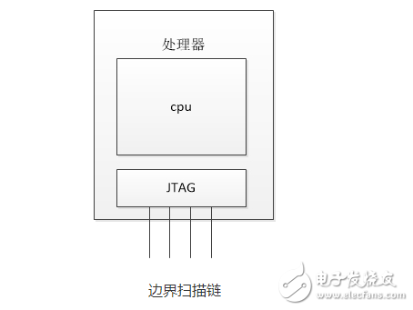
How is JTAG used for chip testing? The most important component used is the boundary scan chain. Named the boundary scan chain because it is located at the boundary of the processor.
We know that the CPU communicates with the peripheral through the pin, all the data will be input or output through the pin, and JTAG achieves the purpose of the chip test by monitoring the signal of the pin. The boundary scan chain is a component on the pin. As shown below:
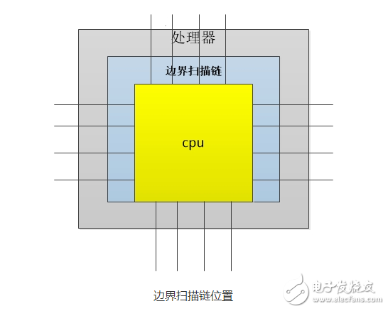
Through the boundary scan chain, when there is a signal input, the boundary scan chain can acquire the signal. When the CPU wants to output the signal, the boundary scan chain can also acquire the signal to be output. Alternatively, the signal can be directly output to the outside through the boundary scan chain.
Whether it's signal capture or output, you need an interface to store these signals. TDI and TDO do just that. Figure:
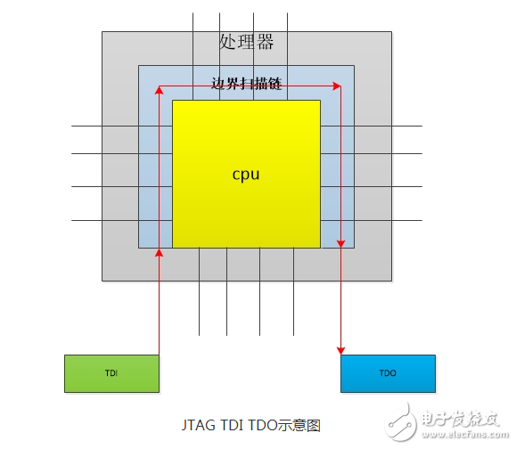
Originally, the boundary scan chain holds the signal on the pin. When we input our own signal through the TDI pin, a shift operation along the red line above occurs.
TDI -> Boundary Scan Chain - 〉 TDO
The signal on the boundary scan chain can be obtained from the TDO, and the signal we input from the TDI will also go to the boundary scan chain.
The data on the pin that the CPU communicates with the outside world is nothing more than the command and data signals (including address and data). But the combination of the two forms a complete program, and monitoring them shows that we can debug the program. A typical chip will provide several independent boundary scan chains. The control of the boundary scan chain is mainly done by the TAP (Test Access Port) Controller.
The above is just the most basic principle of jtag. To better debug the program, you need to control the components, and more combinations of registers.
Laptop Stand Amazon Basics,Laptop Stand Amazon Basics Aluminum,Laptop Stand Amazon Basics Ventilated,Laptop Stand Amazon Choice,etc.
Shenzhen Chengrong Technology Co.ltd is a high-quality enterprise specializing in metal stamping and CNC production for 12 years. The company mainly aims at the R&D, production and sales of Notebook Laptop Stands and Mobile Phone Stands. From the mold design and processing to machining and product surface oxidation, spraying treatment etc ,integration can fully meet the various processing needs of customers. Have a complete and scientific quality management system, strength and product quality are recognized and trusted by the industry, to meet changing economic and social needs .
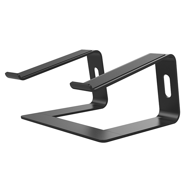
Laptop Stand Amazon Basics,Laptop Stand Amazon Basics Aluminum,Laptop Stand Amazon Basics Ventilated,Laptop Stand Amazon Choice
Shenzhen ChengRong Technology Co.,Ltd. , https://www.laptopstandsuppliers.com
