MEMS Structure Science: Research on Knowledge of Oxygen Sensors
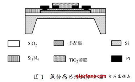
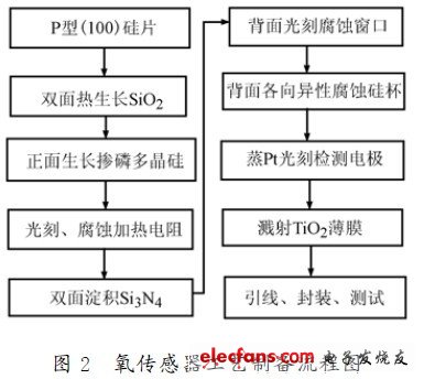
Figure 1 is a schematic illustration of a MEMS structured oxygen sensor. The SiO2 spacer layer is thermally oxidized on a P-type silicon substrate, polycrystalline silicon is grown by an LPCVD apparatus, and a lithographic heating resistor is used. In order to control the resistance of the heating resistor, P is doped into the polysilicon. Then, using the LPCVD method, a Si3 N4 layer is deposited on both sides of the substrate, and a corrosion window is etched on the back side, and the silicon cup is etched by anisotropic etching. Front side steamed Pt lithography to obtain an interdigital detection electrode. Then, a TIO2 sensitive film was grown on the detecting electrode by using an AC magnetron sputtering coating method using a titanium target. It can be seen that the MEMS structure oxygen sensor uses a phosphorus polysilicon resistor under the sensitive film as a heater, and adopts a MEMS deep etching process, thereby reducing the heat capacity of the device and reducing power consumption. The detection electrode and the heating electrode are rationally designed into an integrated device, which can be integrated and mass-produced. The size of the whole chip is 3 mm & TImes; 3mm & TImes; 0.54 mm, the diaphragm thickness is about 2.5 μm, the cup bottom diaphragm size of the silicon cup is 1.4 mm & TImes; 1.4 mm, the sensitive diaphragm size is 0. .72mm × 0.72 mm. The process flow diagram of the MEMS structured TiO2 oxygen sensor is shown in Figure 2.
TiO2 is a wide bandgap semiconductor with a band gap of more than 3 eV. When a TiO2 semiconductor is prepared in a vacuum, when the partial pressure of oxygen is low, a large amount of oxygen vacancies are generated in TiO2 to constitute an N-type semiconductor. The oxygen sensitivity mechanism of the TiO2 film changes as the oxygen vacancy at the center of the donor changes with the partial pressure of the external oxygen, causing a change in the resistivity of the material. The change in oxygen vacancies is achieved by the oxygen adsorption equilibrium on the TiO2 surface. The adsorption process of oxygen on the surface of TiO2 is firstly the physical adsorption of oxygen on the surface of TiO2, then transition to chemisorption, and finally enter the oxygen position of the normal lattice. As the partial pressure of oxygen increases, more and more oxygen is adsorbed by TiO2, and oxygen vacancies are also less and less, so the electric resistance is also gradually increased. Using the mass action relationship, the relationship between the conductivity of titanium dioxide and the partial pressure of oxygen P is: σ = Aμn eP^(- 1/x)
Where: A is the mass action constant, which is the coefficient related to the oxygen vacancy concentration; σ is the conductivity of TiO2; μn is the electron mobility; P is the oxygen partial pressure; with the nature of ion defects and ionization, the value of x is Change between 4 and 6.
The AC magnetron sputtering coating method uses a high-voltage electric field to ionize an inert gas glow discharge under the control of a magnetic field. The positive ions generated by ionization bombard the target at high speed to sputter the titanium atoms on the target, and sputter it. The titanium atom reacts with the reaction gas O2 to deposit a TiO2 film on the substrate.
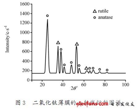
We use a high-purity titanium plate as a target in the JGP-350 magnetron sputtering machine with a diameter of 60 mm, a thickness of 4 mm, a target-to-substrate spacing of 60 mm, and a reactive magnetron sputtering frequency of 13. 56 MHz. The working gas is 99.99% pure Ar and 99.99% O2. A mass flow controller is used to control the flow of the reaction gas O2 while a piezoelectric valve is used to control the working gas pressure in the vacuum chamber. The composite pressure controller is used to control the piezo valve and the vacuum gauge, so that the gas pressure and flow control are very stable. The gas ratio is O2: Ar = 1 : 2 is kept constant. The pre-vacuum of the reaction chamber was 10^(- 3) Pa. The working pressure at the time of sputtering was 70 Pa. The sample substrate is a single crystal silicon wafer, which is ultrasonically cleaned with acetone before coating, and then rinsed and dried with deionized water. The substrate was cooled with water and its temperature was measured with a thermocouple. At this time, an amorphous titanium oxide film was obtained, which was annealed at 500 ° C to obtain anatase titanium dioxide. Figure 3 is an X-ray diffraction pattern (XRD) of a titanium dioxide film prepared by an AC magnetron sputtering coating method. It can be seen from Fig. 3 that the two strongest diffraction peaks appear in the anatase phase (101) crystal plane (2θ = 25 .24°) and (004) crystal plane (2θ = 37.820°), especially ( 101) The preferred orientation of the crystal face is obvious, and the crystallinity increases, indicating that the crystal phase of the surface of the TiO2 film is anatase phase.
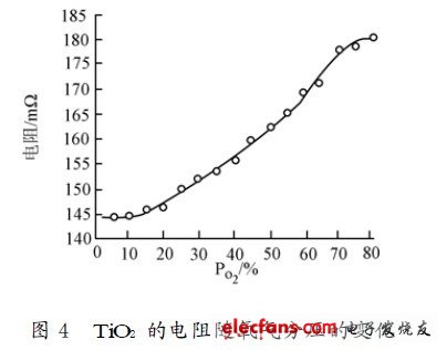
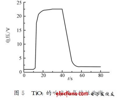
The performance of the resistive oxygen sensitive material is mainly the magnitude of the change in resistance and the response time when the atmosphere changes. The oxygen sensitive performance test of the thin film element can be expressed by detecting a change in resistance when the oxygen content atmosphere changes. Since the resistance of the sense resistor depends only on the volume fraction of oxygen in the gas when the temperature is kept constant, this experiment is to gradually add a certain amount of O2 in a pure N2 atmosphere at room temperature, and then measure the volume of each oxygen. The resistance value of the number. The oxygen sensitivity of the film is shown in Figure 4. It can be seen that the oxygen sensing performance of the thin film component is better, and the variation of the electrical resistance is relatively obvious. Response time is also an important parameter for gas sensing devices. The time required to change the device resistance increment from 33% to 66% of the stable increment is generally defined as response time and recovery time. When a constant current is passed, the voltage value of TiO2 is measured, and the response characteristic of the thin film element shown in Fig. 5 when the atmosphere in the vicinity of the air is repeatedly changed is obtained. It can be seen from the figure that the thin film component has a good response to O2. The response time to the oxygen atmosphere is around 300 ms and the recovery time is around 6 s.
Guangzhou Yunge Tianhong Electronic Technology Co., Ltd , https://www.e-cigarettesfactory.com
